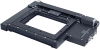
Key features:
Suitable for most major brand microscopes.
2µm or better repeatability
Optional 100nm linear scales provide the highest resolution available.
Wide range of wafer holders
300 mm x 300 mm (12"x12") travel
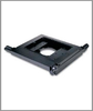
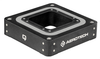
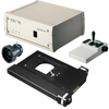
The H112 stage is ideal for scanning a wide range of semiconductor wafers, photo masks, flat panel displays and printed circuit boards. The H112 can easily accommodate 12 inch (300 mm) wafers and works with many robot arm wafer loaders. In addition, the H112 can be used for transmitted light applications with 250 mm x 250 mm transmitted light area.
Key features:
- Suitable for most major brand microscopes.
- 2µm or better repeatability
- Optional 100nm linear scales provide the highest resolution available.
- Wide range of wafer holders
- 300 mm x 300 mm (12"x12") travel
The H112 stage is ideal for scanning a wide range of semiconductor wafers, photo masks, flat panel displays and printed circuit boards. The H112 can easily accommodate 12 inch (300 mm) wafers and works with many robot arm wafer loaders. In addition, the H112 can be used for transmitted light applications with
250 mm x 250 mm transmitted light area.