Overview
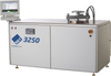
The SST 3250 is a high vacuum multi-atmosphere furnace that has been designed for soldering and bonding components and wafers up to 8-inch (200 mm) diameter. The system is fully operational at vacuum levels of 10-7 Torr and pressures up to 12 psig with automatic selection and control of up to three process gasses.
The 3250’s benefits include:
Closed-loop electronics pressure controller
Integral capacitance manometer for fine control of pressure and flow throughout the full operating range of the system
Uniformity thermal profiles up to 350°C
Processes
Void-Free Die Soldering. Void-free die and substrate solder attach is used to create a uniform thermal interface for high-reliability microelectronic devices. High Vacuum MEMS Package Sealing. Advanced MEMS devices require internal vacuum levels on the order of 1 millitorr over the life of the device. Sealing of these MEMS packages requires specialized thermal processing in high vacuum system.
Hermetic Package Sealing. Hermetic package sealing uses solder or glass to create a barrier to moisture which will damage sensitive electrical circuit components.
Wafer Level Packaging and Wafer Bonding. Wafer Level Packaging (WLP) provides for both interconnection and package sealing of circuits at the wafer level. Processes include flip chip solder reflow, solder lid sealing and wafer-to-wafer bonding using solder, glass, adhesives and direct fusion
Applications
Gated light arrays
MEMS devices
Oscillators
Pressure sensors
Night Vision IR sensors
Miniature crystals
Overview
The SST 3250 is a high vacuum multi-atmosphere furnace that has been designed for soldering and bonding components and wafers up to 8-inch (200 mm) diameter. The system is fully operational at vacuum levels of 10-7 Torr and pressures up to 12 psig with automatic selection and control of up to three process gasses.
The 3250’s benefits include:
- Closed-loop electronics pressure controller
- Integral capacitance manometer for fine control of pressure and flow throughout the full operating range of the system
- Uniformity thermal profiles up to 350°C
Processes
Void-Free Die Soldering. Void-free die and substrate solder attach is used to create a uniform thermal interface for high-reliability microelectronic devices.
High Vacuum MEMS Package Sealing. Advanced MEMS devices require internal vacuum levels on the order of 1 millitorr over the life of the device. Sealing of these MEMS packages requires specialized thermal processing in high vacuum system.
Hermetic Package Sealing. Hermetic package sealing uses solder or glass to create a barrier to moisture which will damage sensitive electrical circuit components.
Wafer Level Packaging and Wafer Bonding. Wafer Level Packaging (WLP) provides for both interconnection and package sealing of circuits at the wafer level. Processes include flip chip solder reflow, solder lid sealing and wafer-to-wafer bonding using solder, glass, adhesives and direct fusion
Applications
- Gated light arrays
- MEMS devices
- Oscillators
- Pressure sensors
- Night Vision IR sensors
- Miniature crystals