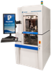

The Palomar 6500 high precision component placement Die Bonder is designed for high-speed, fully automated precision component assembly and offers extraordinary micron-level placement accuracy for photonic, wireless, and medical applications. This eutectic and epoxy die bonder has a 1.5µm placement accuracy, making component assembly practical and cost-effective.
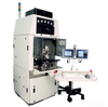
A specialized configuration of the 6500 Die Bonder for wafer scale packaging eutectic die bonding is also available.
Wafer Scale Packaging (WSP)
Wafer Scale Packaging (WSP) eutectic die attach on the 6500 Die Bonder provides customers with a complete microelectronic solution for P-side down laser diode attachment (die-to-wafer), pulsed heat pick tool for 80/20 Au/Sn pulsed reflow attachment, wafer stage with steady state heating, and waffle or gel pack presentation of laser diode applications.
The 6500 Die Bonder for eutectic wafer scale packaging was designed specifically for fully automatic, high-speed, precision P-Side down laser die-to-wafer eutectic assembly.
High-Accuracy Pattern Recognition
An advanced Cognex pattern recognition system uses the lookdown camera to locate the wafer substrate locations and Laser N-side, and enables multiple alignment algorithms including area, point, and edge alignment. This system includes auto focusing with programmable on- and off-axis lighting systems to maximize contrast and accuracy in component placement.
Operating in a true Microsoft Windows Pro-based environment, the wafer scale packaging eutectic 6500 Die Bonder brings unparalleled software flexibility, power, and ease of use to precision hybrid component assembly. The user-friendly interface assists in bonding setup, operation, diagnostics, and calibration.
| Palomar Technologies, Inc | |
|---|---|
| Product Category | Die Bonders |
| Product Number | Palomar 6500 |
| Product Name | Die Bonder |