Nexperia B.V. Low-voltage translating 16-bit I²C-bus/SMBus I/O expander NCA6416BYHP

Description
The NCA6416-Q100 is a versatile 16-bit general-purpose I‌‌/‌‌O expander designed for microcontrollers that need additional I/O pins. It communicates via an I²C-bus interface, making it ideal for applications with minimal space and wiring, such as battery-powered devices using sensors, keypads, push buttons or LED control for managing LED brightness. Nexperia's I/O expanders feature a dual power supply architecture with two inputs: VCCI and VCCP. This design enables seamless level translation, supporting mixed-voltage environments. VCCI powers the I²C interface and must be connected to the same voltage as the host microcontroller's I²C bus (SDA/SCL), which can range from 1.65 V to 5.5 V. VCCP powers the internal core and the I/O pins on Port P, defining the voltage level for the connected peripherals. This allows a low-voltage microcontroller to interface with higher-voltage peripherals without additional external circuitry. The NCA6416-Q100 contains four pairs of 8-bit registers: Configuration, Input, Output, and Polarity Inversion. By default, all I/O pins are configured as inputs at power-on. A system controller can dynamically reconfigure these pins as inputs or outputs by writing to the Configuration register. The Input and Output registers store the current state of each pin. The Polarity Inversion register allows to invert the polarity of the input pins, which can simplify logic in system by eliminating the need for external gates. The device has an open-drain INT output that triggers when an input pin changes state. This interrupt can be connected to a microcontroller's interrupt pin, allowing the NCA6416-Q100 to notify the host of a change without the need for constant polling over the I²C bus. This feature makes the NCA6416-Q100 an efficient and passive I²C target device. To recover from errors like I²C time-outs, a system controller can drive the RESET input low. This resets all registers to their default state and reinitializes the I²C/SMBus interface without requiring a power cycle. A hardware ADDR pin allows to program the device's I²C address, making it possible to use up to two NCA6416-Q100 devices on a single bus. In addition, each output pin on Port P can sink up to 25 mA, making it suitable for directly driving low-current loads like LEDs. Features and benefits I²C-bus to parallel port expander Supply voltage range of 1.65 V to 5.5 V Allows bidirectional voltage-level translation and GPIO expansion between: 1.8 V SCL/SDA and 1.8 V, 2.5 V, 3.3 V or 5 V Port P 2.5 V SCL/SDA and 1.8 V, 2.5 V, 3.3 V or 5 V Port P 3.3 V SCL/SDA and 1.8 V, 2.5 V, 3.3 V or 5 V Port P 5 V SCL/SDA and 1.8 V, 2.5 V, 3.3 V or 5 V Port P Low standby current consumption: 1.5 μA typical at 5 V VCC 1.0 μA typical at 3.3 V VCC Schmitt-trigger action allows slow input transition and better switching noise immunity at the SCL and SDA inputs Vhys = 0.18 V (typical) at 1.8 V Vhys = 0.25 V (typical) at 2.5 V Vhys = 0.33 V (typical) at 3.3 V Vhys = 0.5 V (typical) at 5 V 5 V tolerant I/O ports Active LOW reset input (RESET) Open-drain active LOW interrupt output (INT) 400 kHz Fast-mode I²C-bus Input/Output Configuration register Polarity Inversion register Internal power-on reset Glitch free power-up No power up sequence required Partial power down supported Noise filter on SCL/SDA inputs Latched outputs with 25 mA drive maximum capability for directly driving LEDs Latch-up performance exceeds 100 mA per JESD 78, Class II ESD protection: HBM: ANSI/ESDA/JEDEC JS-001 class 2 exceeds 2000 V CDM: ANSI/ESDA/JEDEC JS-002 class C3 exceeds 1000 V Packages offered: TSSOP24, HWQFN24 Specified from -40 °C to +85 °C and from -40 °C to +125 °C
Request a Quote Datasheet
Description
The NCA6416-Q100 is a versatile 16-bit general-purpose I‌‌/‌‌O expander designed for microcontrollers that need additional I/O pins. It communicates via an I²C-bus interface, making it ideal for applications with minimal space and wiring, such as battery-powered devices using sensors, keypads, push buttons or LED control for managing LED brightness. Nexperia's I/O expanders feature a dual power supply architecture with two inputs: VCCI and VCCP. This design enables seamless level translation, supporting mixed-voltage environments. VCCI powers the I²C interface and must be connected to the same voltage as the host microcontroller's I²C bus (SDA/SCL), which can range from 1.65 V to 5.5 V. VCCP powers the internal core and the I/O pins on Port P, defining the voltage level for the connected peripherals. This allows a low-voltage microcontroller to interface with higher-voltage peripherals without additional external circuitry. The NCA6416-Q100 contains four pairs of 8-bit registers: Configuration, Input, Output, and Polarity Inversion. By default, all I/O pins are configured as inputs at power-on. A system controller can dynamically reconfigure these pins as inputs or outputs by writing to the Configuration register. The Input and Output registers store the current state of each pin. The Polarity Inversion register allows to invert the polarity of the input pins, which can simplify logic in system by eliminating the need for external gates. The device has an open-drain INT output that triggers when an input pin changes state. This interrupt can be connected to a microcontroller's interrupt pin, allowing the NCA6416-Q100 to notify the host of a change without the need for constant polling over the I²C bus. This feature makes the NCA6416-Q100 an efficient and passive I²C target device. To recover from errors like I²C time-outs, a system controller can drive the RESET input low. This resets all registers to their default state and reinitializes the I²C/SMBus interface without requiring a power cycle. A hardware ADDR pin allows to program the device's I²C address, making it possible to use up to two NCA6416-Q100 devices on a single bus. In addition, each output pin on Port P can sink up to 25 mA, making it suitable for directly driving low-current loads like LEDs. Features and benefits I²C-bus to parallel port expander Supply voltage range of 1.65 V to 5.5 V Allows bidirectional voltage-level translation and GPIO expansion between: 1.8 V SCL/SDA and 1.8 V, 2.5 V, 3.3 V or 5 V Port P 2.5 V SCL/SDA and 1.8 V, 2.5 V, 3.3 V or 5 V Port P 3.3 V SCL/SDA and 1.8 V, 2.5 V, 3.3 V or 5 V Port P 5 V SCL/SDA and 1.8 V, 2.5 V, 3.3 V or 5 V Port P Low standby current consumption: 1.5 μA typical at 5 V VCC 1.0 μA typical at 3.3 V VCC Schmitt-trigger action allows slow input transition and better switching noise immunity at the SCL and SDA inputs Vhys = 0.18 V (typical) at 1.8 V Vhys = 0.25 V (typical) at 2.5 V Vhys = 0.33 V (typical) at 3.3 V Vhys = 0.5 V (typical) at 5 V 5 V tolerant I/O ports Active LOW reset input (RESET) Open-drain active LOW interrupt output (INT) 400 kHz Fast-mode I²C-bus Input/Output Configuration register Polarity Inversion register Internal power-on reset Glitch free power-up No power up sequence required Partial power down supported Noise filter on SCL/SDA inputs Latched outputs with 25 mA drive maximum capability for directly driving LEDs Latch-up performance exceeds 100 mA per JESD 78, Class II ESD protection: HBM: ANSI/ESDA/JEDEC JS-001 class 2 exceeds 2000 V CDM: ANSI/ESDA/JEDEC JS-002 class C3 exceeds 1000 V Packages offered: TSSOP24, HWQFN24 Specified from -40 °C to +85 °C and from -40 °C to +125 °C
Request a Quote Datasheet

Suppliers

Company
Product
Description
Supplier Links
Low-voltage translating 16-bit I²C-bus/SMBus I/O expander - NCA6416BYHP - Nexperia B.V.
Nijmegen, Netherlands
Low-voltage translating 16-bit I²C-bus/SMBus I/O expander
NCA6416BYHP
Low-voltage translating 16-bit I²C-bus/SMBus I/O expander NCA6416BYHP
The NCA6416-Q100 is a versatile 16-bit general-purpose I‌‌/‌‌O expander designed for microcontrollers that need additional I/O pins. It communicates via an I²C-bus interface, making it ideal for applications with minimal space and wiring, such as battery-powered devices using sensors, keypads, push buttons or LED control for managing LED brightness. Nexperia's I/O expanders feature a dual power supply architecture with two inputs: VCCI and VCCP. This design enables seamless level translation, supporting mixed-voltage environments. VCCI powers the I²C interface and must be connected to the same voltage as the host microcontroller's I²C bus (SDA/SCL), which can range from 1.65 V to 5.5 V. VCCP powers the internal core and the I/O pins on Port P, defining the voltage level for the connected peripherals. This allows a low-voltage microcontroller to interface with higher-voltage peripherals without additional external circuitry. The NCA6416-Q100 contains four pairs of 8-bit registers: Configuration, Input, Output, and Polarity Inversion. By default, all I/O pins are configured as inputs at power-on. A system controller can dynamically reconfigure these pins as inputs or outputs by writing to the Configuration register. The Input and Output registers store the current state of each pin. The Polarity Inversion register allows to invert the polarity of the input pins, which can simplify logic in system by eliminating the need for external gates. The device has an open-drain INT output that triggers when an input pin changes state. This interrupt can be connected to a microcontroller's interrupt pin, allowing the NCA6416-Q100 to notify the host of a change without the need for constant polling over the I²C bus. This feature makes the NCA6416-Q100 an efficient and passive I²C target device. To recover from errors like I²C time-outs, a system controller can drive the RESET input low. This resets all registers to their default state and reinitializes the I²C/SMBus interface without requiring a power cycle. A hardware ADDR pin allows to program the device's I²C address, making it possible to use up to two NCA6416-Q100 devices on a single bus. In addition, each output pin on Port P can sink up to 25 mA, making it suitable for directly driving low-current loads like LEDs. Features and benefits I²C-bus to parallel port expander Supply voltage range of 1.65 V to 5.5 V Allows bidirectional voltage-level translation and GPIO expansion between: 1.8 V SCL/SDA and 1.8 V, 2.5 V, 3.3 V or 5 V Port P 2.5 V SCL/SDA and 1.8 V, 2.5 V, 3.3 V or 5 V Port P 3.3 V SCL/SDA and 1.8 V, 2.5 V, 3.3 V or 5 V Port P 5 V SCL/SDA and 1.8 V, 2.5 V, 3.3 V or 5 V Port P Low standby current consumption: 1.5 μA typical at 5 V VCC 1.0 μA typical at 3.3 V VCC Schmitt-trigger action allows slow input transition and better switching noise immunity at the SCL and SDA inputs Vhys = 0.18 V (typical) at 1.8 V Vhys = 0.25 V (typical) at 2.5 V Vhys = 0.33 V (typical) at 3.3 V Vhys = 0.5 V (typical) at 5 V 5 V tolerant I/O ports Active LOW reset input (RESET) Open-drain active LOW interrupt output (INT) 400 kHz Fast-mode I²C-bus Input/Output Configuration register Polarity Inversion register Internal power-on reset Glitch free power-up No power up sequence required Partial power down supported Noise filter on SCL/SDA inputs Latched outputs with 25 mA drive maximum capability for directly driving LEDs Latch-up performance exceeds 100 mA per JESD 78, Class II ESD protection: HBM: ANSI/ESDA/JEDEC JS-001 class 2 exceeds 2000 V CDM: ANSI/ESDA/JEDEC JS-002 class C3 exceeds 1000 V Packages offered: TSSOP24, HWQFN24 Specified from -40 °C to +85 °C and from -40 °C to +125 °C
The NCA6416-Q100 is a versatile 16-bit general-purpose I‌‌/‌‌O expander designed for microcontrollers that need additional I/O pins. It communicates via an I²C-bus interface, making it ideal for applications with minimal space and wiring, such as battery-powered devices using sensors, keypads, push buttons or LED control for managing LED brightness.

Nexperia's I/O expanders feature a dual power supply architecture with two inputs: VCCI and VCCP. This design enables seamless level translation, supporting mixed-voltage environments. VCCI powers the I²C interface and must be connected to the same voltage as the host microcontroller's I²C bus (SDA/SCL), which can range from 1.65 V to 5.5 V. VCCP powers the internal core and the I/O pins on Port P, defining the voltage level for the connected peripherals. This allows a low-voltage microcontroller to interface with higher-voltage peripherals without additional external circuitry.

The NCA6416-Q100 contains four pairs of 8-bit registers: Configuration, Input, Output, and Polarity Inversion. By default, all I/O pins are configured as inputs at power-on. A system controller can dynamically reconfigure these pins as inputs or outputs by writing to the Configuration register. The Input and Output registers store the current state of each pin. The Polarity Inversion register allows to invert the polarity of the input pins, which can simplify logic in system by eliminating the need for external gates.

The device has an open-drain INT output that triggers when an input pin changes state. This interrupt can be connected to a microcontroller's interrupt pin, allowing the NCA6416-Q100 to notify the host of a change without the need for constant polling over the I²C bus. This feature makes the NCA6416-Q100 an efficient and passive I²C target device.

To recover from errors like I²C time-outs, a system controller can drive the RESET input low. This resets all registers to their default state and reinitializes the I²C/SMBus interface without requiring a power cycle.

A hardware ADDR pin allows to program the device's I²C address, making it possible to use up to two NCA6416-Q100 devices on a single bus.

In addition, each output pin on Port P can sink up to 25 mA, making it suitable for directly driving low-current loads like LEDs.

Features and benefits

  • I²C-bus to parallel port expander
  • Supply voltage range of 1.65 V to 5.5 V
  • Allows bidirectional voltage-level translation and GPIO expansion between:
    • 1.8 V SCL/SDA and 1.8 V, 2.5 V, 3.3 V or 5 V Port P
    • 2.5 V SCL/SDA and 1.8 V, 2.5 V, 3.3 V or 5 V Port P
    • 3.3 V SCL/SDA and 1.8 V, 2.5 V, 3.3 V or 5 V Port P
    • 5 V SCL/SDA and 1.8 V, 2.5 V, 3.3 V or 5 V Port P
  • Low standby current consumption:
    • 1.5 μA typical at 5 V VCC
    • 1.0 μA typical at 3.3 V VCC
  • Schmitt-trigger action allows slow input transition and better switching noise immunity at the SCL and SDA inputs
    • Vhys = 0.18 V (typical) at 1.8 V
    • Vhys = 0.25 V (typical) at 2.5 V
    • Vhys = 0.33 V (typical) at 3.3 V
    • Vhys = 0.5 V (typical) at 5 V
  • 5 V tolerant I/O ports
  • Active LOW reset input (RESET)
  • Open-drain active LOW interrupt output (INT)
  • 400 kHz Fast-mode I²C-bus
  • Input/Output Configuration register
  • Polarity Inversion register
  • Internal power-on reset
  • Glitch free power-up
  • No power up sequence required
  • Partial power down supported
  • Noise filter on SCL/SDA inputs
  • Latched outputs with 25 mA drive maximum capability for directly driving LEDs
  • Latch-up performance exceeds 100 mA per JESD 78, Class II
  • ESD protection:
    • HBM: ANSI/ESDA/JEDEC JS-001 class 2 exceeds 2000 V
    • CDM: ANSI/ESDA/JEDEC JS-002 class C3 exceeds 1000 V
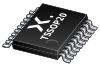
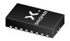
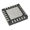
  • Packages offered: TSSOP24, HWQFN24
  • Specified from -40 °C to +85 °C and from -40 °C to +125 °C
Supplier's Site Datasheet
I/O Expanders - 1727-NCA6416BYHPDKR-ND - DigiKey
Thief River Falls, MN, United States
NCA6416BY/SOT8041/HW QFN24

NCA6416BY/SOT8041/HWQFN24

Buy Now Datasheet
I/O Expanders - 1727-NCA6416BYHPCT-ND - DigiKey
Thief River Falls, MN, United States
NCA6416BY/SOT8041/HW QFN24

NCA6416BY/SOT8041/HWQFN24

Buy Now Datasheet
I/O Expanders - 1727-NCA6416BYHPTR-ND - DigiKey
Thief River Falls, MN, United States
NCA6416BY/SOT8041/HW QFN24

NCA6416BY/SOT8041/HWQFN24

Buy Now Datasheet

Technical Specifications

  Nexperia B.V. DigiKey
Product Category IC Interfaces IC Interfaces
Product Number NCA6416BYHP 1727-NCA6416BYHPDKR-ND
Product Name Low-voltage translating 16-bit I²C-bus/SMBus I/O expander I/O Expanders
Technology CMOS I2C; SMBus
Features RoHS
Supply Voltage 1.8V; 2.5V; 2.7V; 3V; 3.3V; 3.6V; 5V; Other; 1.65 - 5.5 Other; 1.65V ~ 5.5V
Operating Temperature -40 to 85 C (-40 to 185 F) -40 to 125 C (-40 to 257 F)
Unlock Full Specs
to access all available technical data

Similar Products

Bus buffer/line driver; 3-state - 74AHCT1G125GW,118 - Nexperia B.V.
Specs
Technology TTL
Device Type Buffer
Supply Voltage 5V; Other; 4.5 - 5.5
View Details
Hex buffer/line driver; 3-state - 74HC367D,652 - Nexperia B.V.
Specs
Technology CMOS
Device Type Buffer
Supply Voltage 2.5V; 2.7V; 3V; 3.3V; 3.6V; 5V; Other; 2.0 - 6.0
View Details
3 suppliers
Buffer with open-drain output - 74AHC1G07GZYL - Nexperia B.V.
Specs
Technology CMOS
Device Type Buffer
Features RoHS
View Details
16-bit buffer/line driver with 30 Ohm series termination resistors; 3-state - 74ABT162244DGG,118 - Nexperia B.V.
Specs
Technology TTL
Device Type Buffer
Features RoHS
View Details
2 suppliers