The 74VHC08; 74VHCT08 are high-speed Si-gate CMOS devices and are pin compatible with Low-power Schottky TTL (LSTTL). They are specified in compliance with JEDEC standard JESD7-A.
The 74VHC08; 74VHCT08 provide the quad 2-input AND function.
Features and benefits
Balanced propagation delays
All inputs have a Schmitt-trigger action
Inputs accepts voltages higher than VCC
Input levels:
The 74VHC08 operates with CMOS logic levels
The 74VHCT08 operates with TTL logic levels
ESD protection:
HBM: ANSI/ESDA/JEDEC JS-001 class 2 exceeds 2000 V
CDM: ANSI/ESDA/JEDEC JS-002 class C3 exceeds 1000 V
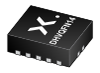
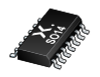
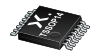
Multiple package options
Specified from -40 °C to +85 °C and from -40 °C to +125 °C
The 74VHC08; 74VHCT08 are high-speed Si-gate CMOS devices and are pin compatible with Low-power Schottky TTL (LSTTL). They are specified in compliance with JEDEC standard JESD7-A.
The 74VHC08; 74VHCT08 provide the quad 2-input AND function.
Features and benefits
- Balanced propagation delays
- All inputs have a Schmitt-trigger action
- Inputs accepts voltages higher than VCC
- Input levels:
- The 74VHC08 operates with CMOS logic levels
- The 74VHCT08 operates with TTL logic levels
- ESD protection:
- HBM: ANSI/ESDA/JEDEC JS-001 class 2 exceeds 2000 V
- CDM: ANSI/ESDA/JEDEC JS-002 class C3 exceeds 1000 V
- Multiple package options
- Specified from -40 °C to +85 °C and from -40 °C to +125 °C