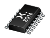
The 74LVC573A-Q100 is an 8-bit D-type transparent latch with 3-state outputs. The device features latch enable (LE) and output enable (OE) inputs. When LE is HIGH, data at the inputs enter the latches. In this condition the latches are transparent, a latch output will change each time its corresponding D-input changes. When LE is LOW the latches store the information that was present at the inputs a set-up time preceding the HIGH-to-LOW transition of LE. A HIGH on OEcauses the outputs to assume a high-impedance OFF-state. Operation of the OEinput does not affect the state of the latches. Inputs can be driven from either 3.3 V or 5 V devices. This feature allows the use of these devices as translators in mixed 3.3 V and 5 V environments.
Schmitt-trigger action at all inputs makes the circuit tolerant of slower input rise and fall times.
This device is fully specified for partial power down applications using IOFF. The IOFF circuitry disables the output, preventing the potentially damaging backflow current through the device when it is powered down.
This product has been qualified to the Automotive Electronics Council (AEC) standard Q100 (Grade 1) and is suitable for use in automotive applications.
Features and benefits
Automotive product qualification in accordance with AEC-Q100 (Grade 1)
Specified from -40 °C to +85 °C and from -40 °C to +125 °C
Wide supply voltage range from 1.2 to 3.6 V
Overvoltage tolerant inputs to 5.5 V
CMOS low power consumption
Direct interface with TTL levels
IOFF circuitry provides partial Power-down mode operation
High-impedance when VCC = 0 V
Flow-through pinout architecture
Complies with JEDEC standard:
JESD8-7A (1.65 V to 1.95 V)
JESD8-5A (2.3 V to 2.7 V)
JESD8-C/JESD36 (2.7 V to 3.6 V)
ESD protection:
HBM: ANSI/ESDA/JEDEC JS-001 class 2 exceeds 2000 V
CDM: ANSI/ESDA/JEDEC JS-002 class C3 exceeds 1000 V
DHVQFN package with Side-Wettable Flanks enabling Automated Optical Inspection (AOI) of solder joints
The 74LVC573A-Q100 is an 8-bit D-type transparent latch with 3-state outputs. The device features latch enable (LE) and output enable (OE) inputs. When LE is HIGH, data at the inputs enter the latches. In this condition the latches are transparent, a latch output will change each time its corresponding D-input changes. When LE is LOW the latches store the information that was present at the inputs a set-up time preceding the HIGH-to-LOW transition of LE. A HIGH on OEcauses the outputs to assume a high-impedance OFF-state. Operation of the OEinput does not affect the state of the latches. Inputs can be driven from either 3.3 V or 5 V devices. This feature allows the use of these devices as translators in mixed 3.3 V and 5 V environments.
Schmitt-trigger action at all inputs makes the circuit tolerant of slower input rise and fall times.
This device is fully specified for partial power down applications using IOFF. The IOFF circuitry disables the output, preventing the potentially damaging backflow current through the device when it is powered down.
This product has been qualified to the Automotive Electronics Council (AEC) standard Q100 (Grade 1) and is suitable for use in automotive applications.
Features and benefits
- Automotive product qualification in accordance with AEC-Q100 (Grade 1)
- Specified from -40 °C to +85 °C and from -40 °C to +125 °C
- Wide supply voltage range from 1.2 to 3.6 V
- Overvoltage tolerant inputs to 5.5 V
- CMOS low power consumption
- Direct interface with TTL levels
- IOFF circuitry provides partial Power-down mode operation
- High-impedance when VCC = 0 V
- Flow-through pinout architecture
- Complies with JEDEC standard:
- JESD8-7A (1.65 V to 1.95 V)
- JESD8-5A (2.3 V to 2.7 V)
- JESD8-C/JESD36 (2.7 V to 3.6 V)
- ESD protection:
- HBM: ANSI/ESDA/JEDEC JS-001 class 2 exceeds 2000 V
- CDM: ANSI/ESDA/JEDEC JS-002 class C3 exceeds 1000 V
- DHVQFN package with Side-Wettable Flanks enabling Automated Optical Inspection (AOI) of solder joints