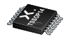
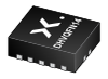
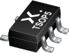
The 74LVC4T3144 is a 4-bit, dual-supply level translating buffer with 3-state outputs. It features four data inputs (An and B4), four data outputs (YBn and YA4), and an output enable input (OE). The device is configured to translate three inputs from VCC(A) to VCC(B) and one input from VCC(B) to VCC(A). OE, An and YA4 are referenced to VCC(A) and YBn and B4 are referenced to VCC(B). A HIGH on OEcauses the outputs to assume a high-impedance OFF-state.
The device is fully specified for partial power-down applications using IOFF. The IOFF circuitry disables outputs, preventing any damaging backflow current through the device when it is powered down. In suspend mode when either VCC(A) or VCC(B) are at GND level, all outputs are in the high-impedance OFF-state.
Features and benefits
Wide supply voltage range:
VCC(A): 1.2 V to 5.5 V
VCC(B): 1.2 V to 5.5 V
High noise immunity
Maximum data rates:
200 Mbps (3.3 V to 5.0 V translation)
140 Mbps (translate to 3.3 V))
100 Mbps (translate to 2.5 V)
75 Mbps (translate to 1.8 V)
60 Mbps (translate to 1.5 V)
Suspend mode
Latch-up performance exceeds 100 mA per JESD 78B Class II
±24 mA output drive (VCC = 3.0 V)
Inputs accept voltages up to 5.5 V
Low power consumption: 30 μA maximum ICC
IOFF circuitry provides partial Power-down mode operation
Complies with JEDEC standards:
JESD8-11A (1.4 V to 1.6 V)
JESD8-7 (1.65 V to 1.95 V)
JESD8-5 (2.3 V to 2.7 V)
JESD8C (3.0 V to 3.6 V)
JESD12-6 (4.5 V to 5.5 V)
ESD protection:
HBM: ANSI/ESDA/JEDEC JS-001 class 2 exceeds 2000 V
CDM: ANSI/ESDA/JEDEC JS-002 class C3 exceeds 1000 V
Specified from -40 °C to +85 °C and -40 °C to +125 °C
The 74LVC4T3144 is a 4-bit, dual-supply level translating buffer with 3-state outputs. It features four data inputs (An and B4), four data outputs (YBn and YA4), and an output enable input (OE). The device is configured to translate three inputs from VCC(A) to VCC(B) and one input from VCC(B) to VCC(A). OE, An and YA4 are referenced to VCC(A) and YBn and B4 are referenced to VCC(B). A HIGH on OEcauses the outputs to assume a high-impedance OFF-state.
The device is fully specified for partial power-down applications using IOFF. The IOFF circuitry disables outputs, preventing any damaging backflow current through the device when it is powered down. In suspend mode when either VCC(A) or VCC(B) are at GND level, all outputs are in the high-impedance OFF-state.
Features and benefits
- Wide supply voltage range:
- VCC(A): 1.2 V to 5.5 V
- VCC(B): 1.2 V to 5.5 V
- High noise immunity
- Maximum data rates:
- 200 Mbps (3.3 V to 5.0 V translation)
- 140 Mbps (translate to 3.3 V))
- 100 Mbps (translate to 2.5 V)
- 75 Mbps (translate to 1.8 V)
- 60 Mbps (translate to 1.5 V)
- Suspend mode
- Latch-up performance exceeds 100 mA per JESD 78B Class II
- ±24 mA output drive (VCC = 3.0 V)
- Inputs accept voltages up to 5.5 V
- Low power consumption: 30 μA maximum ICC
- IOFF circuitry provides partial Power-down mode operation
- Complies with JEDEC standards:
- JESD8-11A (1.4 V to 1.6 V)
- JESD8-7 (1.65 V to 1.95 V)
- JESD8-5 (2.3 V to 2.7 V)
- JESD8C (3.0 V to 3.6 V)
- JESD12-6 (4.5 V to 5.5 V)
- ESD protection:
- HBM: ANSI/ESDA/JEDEC JS-001 class 2 exceeds 2000 V
- CDM: ANSI/ESDA/JEDEC JS-002 class C3 exceeds 1000 V
- Specified from -40 °C to +85 °C and -40 °C to +125 °C