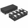
Nexperia B.V. Triple buffer 74LVC3G34GS,115

Description
The 74LVC3G34 is a triple buffer. Inputs can be driven from either 3.3 V or 5 V devices. This feature allows the use of these devices as translators in mixed 3.3 V and 5 V environments. Schmitt-trigger action at all inputs makes the circuit tolerant of slower input rise and fall times. This device is fully specified for partial power down applications using IOFF. The IOFF circuitry disables the output, preventing the potentially damaging backflow current through the device when it is powered down. Features and benefits Wide supply voltage range from 1.65 V to 5.5 V Overvoltage tolerant inputs to 5.5 V High noise immunity ±24 mA output drive (VCC = 3.0 V) CMOS low power consumption Latch-up performance exceeds 250 mA Direct interface with TTL levels Complies with JEDEC standard: JESD8-7 (1.65 V to 1.95 V) JESD8-5 (2.3 V to 2.7 V) JESD8C (2.7 V to 3.6 V) JESD36 (4.5 V to 5.5 V) ESD protection: HBM: ANSI/ESDA/JEDEC JS-001 class 2 exceeds 2000 V CDM: ANSI/ESDA/JEDEC JS-002 class C3 exceeds 1000 V Multiple package options Specified from -40 °C to +85 °C and -40 °C to +125 °C
Request a Quote Datasheet
Description
The 74LVC3G34 is a triple buffer. Inputs can be driven from either 3.3 V or 5 V devices. This feature allows the use of these devices as translators in mixed 3.3 V and 5 V environments. Schmitt-trigger action at all inputs makes the circuit tolerant of slower input rise and fall times. This device is fully specified for partial power down applications using IOFF. The IOFF circuitry disables the output, preventing the potentially damaging backflow current through the device when it is powered down. Features and benefits Wide supply voltage range from 1.65 V to 5.5 V Overvoltage tolerant inputs to 5.5 V High noise immunity ±24 mA output drive (VCC = 3.0 V) CMOS low power consumption Latch-up performance exceeds 250 mA Direct interface with TTL levels Complies with JEDEC standard: JESD8-7 (1.65 V to 1.95 V) JESD8-5 (2.3 V to 2.7 V) JESD8C (2.7 V to 3.6 V) JESD36 (4.5 V to 5.5 V) ESD protection: HBM: ANSI/ESDA/JEDEC JS-001 class 2 exceeds 2000 V CDM: ANSI/ESDA/JEDEC JS-002 class C3 exceeds 1000 V Multiple package options Specified from -40 °C to +85 °C and -40 °C to +125 °C
Request a Quote Datasheet

Suppliers

Company
Product
Description
Supplier Links
Triple buffer - 74LVC3G34GS,115 - Nexperia B.V.
Nijmegen, Netherlands
Triple buffer
74LVC3G34GS,115
Triple buffer 74LVC3G34GS,115
The 74LVC3G34 is a triple buffer. Inputs can be driven from either 3.3 V or 5 V devices. This feature allows the use of these devices as translators in mixed 3.3 V and 5 V environments. Schmitt-trigger action at all inputs makes the circuit tolerant of slower input rise and fall times. This device is fully specified for partial power down applications using IOFF. The IOFF circuitry disables the output, preventing the potentially damaging backflow current through the device when it is powered down. Features and benefits Wide supply voltage range from 1.65 V to 5.5 V Overvoltage tolerant inputs to 5.5 V High noise immunity ±24 mA output drive (VCC = 3.0 V) CMOS low power consumption Latch-up performance exceeds 250 mA Direct interface with TTL levels Complies with JEDEC standard: JESD8-7 (1.65 V to 1.95 V) JESD8-5 (2.3 V to 2.7 V) JESD8C (2.7 V to 3.6 V) JESD36 (4.5 V to 5.5 V) ESD protection: HBM: ANSI/ESDA/JEDEC JS-001 class 2 exceeds 2000 V CDM: ANSI/ESDA/JEDEC JS-002 class C3 exceeds 1000 V Multiple package options Specified from -40 °C to +85 °C and -40 °C to +125 °C

The 74LVC3G34 is a triple buffer. Inputs can be driven from either 3.3 V or 5 V devices. This feature allows the use of these devices as translators in mixed 3.3 V and 5 V environments.

Schmitt-trigger action at all inputs makes the circuit tolerant of slower input rise and fall times.

This device is fully specified for partial power down applications using IOFF. The IOFF circuitry disables the output, preventing the potentially damaging backflow current through the device when it is powered down.

Features and benefits

  • Wide supply voltage range from 1.65 V to 5.5 V
  • Overvoltage tolerant inputs to 5.5 V
  • High noise immunity
  • ±24 mA output drive (VCC = 3.0 V)
  • CMOS low power consumption
  • Latch-up performance exceeds 250 mA
  • Direct interface with TTL levels
  • Complies with JEDEC standard:
    • JESD8-7 (1.65 V to 1.95 V)
    • JESD8-5 (2.3 V to 2.7 V)
    • JESD8C (2.7 V to 3.6 V)
    • JESD36 (4.5 V to 5.5 V)
  • ESD protection:
    • HBM: ANSI/ESDA/JEDEC JS-001 class 2 exceeds 2000 V
    • CDM: ANSI/ESDA/JEDEC JS-002 class C3 exceeds 1000 V
  • Multiple package options
  • Specified from -40 °C to +85 °C and -40 °C to +125 °C
Supplier's Site Datasheet
5.5V Interface Transceiver IC - 704-74LVC3G34GS,115 - ERSAELECTRONICS PTE. LTD.
Singapore, Singapore
5.5V Interface Transceiver IC
704-74LVC3G34GS,115
5.5V Interface Transceiver IC 704-74LVC3G34GS,115
IC BUFFER NON-INVERT 5.5V 8XSON Product overview: 74LVC3G34GS,115 from Nexperia is an Interface Transceiver IC for serial communication, bus conversion, signal driving, receiver stages, and industrial networking. It is useful for engineers and buyers comparing datasheets, replacement parts, BOM lines, package options, lifecycle status, and procurement availability. Key searchable attributes include 5.5V. Search-friendly keywords include interface IC, transceiver, driver, receiver, CAN, RS-485, 5.5V, Interface Transceiver IC, Buffers, Drivers, Receivers, Transceivers. This listing supports clearer product discovery for industrial, commercial, repair, automation, power, sensing, and embedded system projects. Product number 704-74LVC3G34GS,115 can be used for catalog matching and distributor lookup.

IC BUFFER NON-INVERT 5.5V 8XSON Product overview: 74LVC3G34GS,115 from Nexperia is an Interface Transceiver IC for serial communication, bus conversion, signal driving, receiver stages, and industrial networking. It is useful for engineers and buyers comparing datasheets, replacement parts, BOM lines, package options, lifecycle status, and procurement availability. Key searchable attributes include 5.5V. Search-friendly keywords include interface IC, transceiver, driver, receiver, CAN, RS-485, 5.5V, Interface Transceiver IC, Buffers, Drivers, Receivers, Transceivers. This listing supports clearer product discovery for industrial, commercial, repair, automation, power, sensing, and embedded system projects. Product number 704-74LVC3G34GS,115 can be used for catalog matching and distributor lookup.

Supplier's Site Datasheet

Technical Specifications

  Nexperia B.V. ERSAELECTRONICS PTE. LTD.
Product Category IC Interfaces IC Interfaces
Product Number 74LVC3G34GS,115 704-74LVC3G34GS,115
Product Name Triple buffer 5.5V Interface Transceiver IC
Device Type Buffer Transceiver
Features RoHS RoHS
Supply Voltage Other; +6.5 Other; 1.65V ~ 5.5V
Operating Temperature 125 C (257 F) -40 C (-40 F)
Unlock Full Specs
to access all available technical data

Similar Products

Hex inverting Schmitt trigger - 74AHC14BQ-Q100,115 - Nexperia B.V.
Specs
Features RoHS
Supply Voltage Other; +7.0
Package Type SOT762-1 SOT762-1
View Details
16-bit bus transceiver; 3-state - 74ABT16245BDGG,118 - Nexperia B.V.
Specs
Device Type Transceiver
Features RoHS
Supply Voltage Other; +7.0
View Details
2 suppliers
Specs
Device Type Transceiver
Features RoHS
Supply Voltage Other; 1.2V ~ 3.6V
View Details
Universal Bus Functions - 74ALVT16601DGG,118 - Quarktwin Technology Ltd.
Specs
Device Type Line / Bus Controller
Features RoHS
Supply Voltage 3V; 3.6V; Other; 2.3V ~ 2.7V, 3V ~ 3.6V
View Details