Nexperia B.V. Triple buffer 74LVC3G16DPH

Description
The 74LVC3G16 provides three buffers. The inputs can be driven from either 3.3 V or 5 V devices. This feature allows the use of the 74LVC3G16 as a translator in a mixed 3.3 V and 5 V environment. This device is fully specified for partial power-down applications using IOFF. The IOFF circuitry disables the output, preventing a damaging backflow current through the device when it is powered down. Features and benefits Wide supply voltage range from 1.65 V to 5.5 V 5 V tolerant input/output for interfacing with 5 V logic High noise immunity ±24 mA output drive (VCC = 3.0 V) CMOS low power consumption Latch-up performance exceeds 250 mA Direct interface with TTL levels Complies with JEDEC standard: JESD8-7 (1.65 V to 1.95 V) JESD8-5 (2.3 V to 2.7 V) JESD8B/JESD36 (2.7 V to 3.6 V) ESD protection: HBM: ANSI/ESDA/JEDEC JS-001 class 2 exceeds 2000 V CDM: ANSI/ESDA/JEDEC JS-002 class C3 exceeds 1000 V Specified from -40 °C to +85 °C and -40 °C to +125 °C
Request a Quote Datasheet
Description
The 74LVC3G16 provides three buffers. The inputs can be driven from either 3.3 V or 5 V devices. This feature allows the use of the 74LVC3G16 as a translator in a mixed 3.3 V and 5 V environment. This device is fully specified for partial power-down applications using IOFF. The IOFF circuitry disables the output, preventing a damaging backflow current through the device when it is powered down. Features and benefits Wide supply voltage range from 1.65 V to 5.5 V 5 V tolerant input/output for interfacing with 5 V logic High noise immunity ±24 mA output drive (VCC = 3.0 V) CMOS low power consumption Latch-up performance exceeds 250 mA Direct interface with TTL levels Complies with JEDEC standard: JESD8-7 (1.65 V to 1.95 V) JESD8-5 (2.3 V to 2.7 V) JESD8B/JESD36 (2.7 V to 3.6 V) ESD protection: HBM: ANSI/ESDA/JEDEC JS-001 class 2 exceeds 2000 V CDM: ANSI/ESDA/JEDEC JS-002 class C3 exceeds 1000 V Specified from -40 °C to +85 °C and -40 °C to +125 °C
Request a Quote Datasheet

Suppliers

Company
Product
Description
Supplier Links
Triple buffer - 74LVC3G16DPH - Nexperia B.V.
Nijmegen, Netherlands
Triple buffer
74LVC3G16DPH
Triple buffer 74LVC3G16DPH
The 74LVC3G16 provides three buffers. The inputs can be driven from either 3.3 V or 5 V devices. This feature allows the use of the 74LVC3G16 as a translator in a mixed 3.3 V and 5 V environment. This device is fully specified for partial power-down applications using IOFF. The IOFF circuitry disables the output, preventing a damaging backflow current through the device when it is powered down. Features and benefits Wide supply voltage range from 1.65 V to 5.5 V 5 V tolerant input/output for interfacing with 5 V logic High noise immunity ±24 mA output drive (VCC = 3.0 V) CMOS low power consumption Latch-up performance exceeds 250 mA Direct interface with TTL levels Complies with JEDEC standard: JESD8-7 (1.65 V to 1.95 V) JESD8-5 (2.3 V to 2.7 V) JESD8B/JESD36 (2.7 V to 3.6 V) ESD protection: HBM: ANSI/ESDA/JEDEC JS-001 class 2 exceeds 2000 V CDM: ANSI/ESDA/JEDEC JS-002 class C3 exceeds 1000 V Specified from -40 °C to +85 °C and -40 °C to +125 °C

The 74LVC3G16 provides three buffers.

The inputs can be driven from either 3.3 V or 5 V devices. This feature allows the use of the 74LVC3G16 as a translator in a mixed 3.3 V and 5 V environment.

This device is fully specified for partial power-down applications using IOFF. The IOFF circuitry disables the output, preventing a damaging backflow current through the device when it is powered down.

Features and benefits

  • Wide supply voltage range from 1.65 V to 5.5 V
  • 5 V tolerant input/output for interfacing with 5 V logic
  • High noise immunity
  • ±24 mA output drive (VCC = 3.0 V)
  • CMOS low power consumption
  • Latch-up performance exceeds 250 mA
  • Direct interface with TTL levels
  • Complies with JEDEC standard:
    • JESD8-7 (1.65 V to 1.95 V)
    • JESD8-5 (2.3 V to 2.7 V)
    • JESD8B/JESD36 (2.7 V to 3.6 V)
  • ESD protection:
    • HBM: ANSI/ESDA/JEDEC JS-001 class 2 exceeds 2000 V
    • CDM: ANSI/ESDA/JEDEC JS-002 class C3 exceeds 1000 V
  • Specified from -40 °C to +85 °C and -40 °C to +125 °C
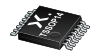
Supplier's Site Datasheet

Technical Specifications

  Nexperia B.V.
Product Category IC Interfaces
Product Number 74LVC3G16DPH
Product Name Triple buffer
Device Type Buffer
Unlock Full Specs
to access all available technical data

Similar Products

Octal buffer/line driver; 3-state - 74AHC244PW,118 - Nexperia B.V.
Specs
Device Type Buffer
Features RoHS
Supply Voltage Other; +7.0
View Details
3 suppliers
Inverter - 74AHCT1G04GM,132 - Nexperia B.V.
Specs
Features RoHS
Supply Voltage Other; +7.0
Package Type SOT886 SOT886
View Details
Buffer with open-drain output - 74AHC1G07GV,125 - Nexperia B.V.
Specs
Device Type Buffer
Features RoHS
Supply Voltage Other; +7.0
View Details
2 suppliers
Quad buffer/line driver; 3-state - 74AHCT125BQ-Q100,1 - Nexperia B.V.
Specs
Device Type Buffer
Features RoHS
Supply Voltage Other; +7.0
View Details