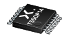
Nexperia B.V. 4-bit bus switch 74CBTLV3125PW-Q10J

Description
The 74CBTLV3125-Q100 provides a 4-bit high-speed bus switch with separate output enable inputs (1OEto 4OE). The low on-state resistance of the switch allows connections to be made with minimal propagation delay. The switch is disabled (high-impedance OFF-state) when the output enable (nOE) input is HIGH. To ensure the high-impedance OFF-state during power-up or power-down, nOEshould be tied to the VCC through a pull-up resistor. The minimum value of the resistor is determined by the current-sinking capability of the driver. Schmitt trigger action at control input makes the circuit tolerant to slower input rise and fall times across the entire VCC range from 2.3 V to 3.6 V. This device is fully specified for partial power-down applications using IOFF. The IOFF circuitry disables the output, preventing the damaging backflow current through the device when it is powered down. This product has been qualified to the Automotive Electronics Council (AEC) standard Q100 (Grade 1) and is suitable for use in automotive applications. Features and benefits Automotive product qualification in accordance with AEC-Q100 (Grade 1) Specified from -40 °C to +85 °C and from -40 °C to +125 °C Supply voltage range from 2.3 V to 3.6 V High noise immunity Complies with JEDEC standard: JESD8-5 (2.3 V to 2.7 V) JESD8-B/JESD36 (2.7 V to 3.6 V) 5 Ω switch connection between two ports Rail to rail switching on data I/O ports CMOS low power consumption Latch-up performance exceeds 250 mA per JESD78B Class I level A IOFF circuitry provides partial Power-down mode operation DHVQFN package with Side-Wettable Flanks enabling Automatic Optical Inspection (AOI) of solder joints ESD protection: HBM: ANSI/ESDA/JEDEC JS-001 class 2 exceeds 2000 V CDM: ANSI/ESDA/JEDEC JS-002 class C3 exceeds 1000 V
Request a Quote
Description
The 74CBTLV3125-Q100 provides a 4-bit high-speed bus switch with separate output enable inputs (1OEto 4OE). The low on-state resistance of the switch allows connections to be made with minimal propagation delay. The switch is disabled (high-impedance OFF-state) when the output enable (nOE) input is HIGH. To ensure the high-impedance OFF-state during power-up or power-down, nOEshould be tied to the VCC through a pull-up resistor. The minimum value of the resistor is determined by the current-sinking capability of the driver. Schmitt trigger action at control input makes the circuit tolerant to slower input rise and fall times across the entire VCC range from 2.3 V to 3.6 V. This device is fully specified for partial power-down applications using IOFF. The IOFF circuitry disables the output, preventing the damaging backflow current through the device when it is powered down. This product has been qualified to the Automotive Electronics Council (AEC) standard Q100 (Grade 1) and is suitable for use in automotive applications. Features and benefits Automotive product qualification in accordance with AEC-Q100 (Grade 1) Specified from -40 °C to +85 °C and from -40 °C to +125 °C Supply voltage range from 2.3 V to 3.6 V High noise immunity Complies with JEDEC standard: JESD8-5 (2.3 V to 2.7 V) JESD8-B/JESD36 (2.7 V to 3.6 V) 5 Ω switch connection between two ports Rail to rail switching on data I/O ports CMOS low power consumption Latch-up performance exceeds 250 mA per JESD78B Class I level A IOFF circuitry provides partial Power-down mode operation DHVQFN package with Side-Wettable Flanks enabling Automatic Optical Inspection (AOI) of solder joints ESD protection: HBM: ANSI/ESDA/JEDEC JS-001 class 2 exceeds 2000 V CDM: ANSI/ESDA/JEDEC JS-002 class C3 exceeds 1000 V
Request a Quote
Datasheet
Datasheet Summary
Powered by GS/AI

The 74CBTLV3125PW-Q100 is a 4-bit high-speed bus switch with separate output enable inputs, designed for automotive applications. It is packaged in a TSSOP14 plastic thin shrink small outline package with a body width of 4.4 mm. The device operates over a supply voltage range of 2.3 V to 3.6 V and is specified for temperature ranges from -40 °C to +125 °C. It features a 5 Ω on-state resistance, rail-to-rail switching, and I₋₟ circuitry for partial power-down operation. The part is qualified to AEC-Q100 (Grade 1), complies with JESD8-5 and JESD8-B/JESD36 standards, and offers ESD protection exceeding 2000 V (HBM) and 1000 V (CDM).

Datasheet Summary
Powered by GS/AI

The 74CBTLV3125PW-Q100 is a 4-bit high-speed bus switch with separate output enable inputs, designed for automotive applications. It is packaged in a TSSOP14 plastic thin shrink small outline package with a body width of 4.4 mm. The device operates over a supply voltage range of 2.3 V to 3.6 V and is specified for temperature ranges from -40 °C to +125 °C. It features a 5 Ω on-state resistance, rail-to-rail switching, and I₋₟ circuitry for partial power-down operation. The part is qualified to AEC-Q100 (Grade 1), complies with JESD8-5 and JESD8-B/JESD36 standards, and offers ESD protection exceeding 2000 V (HBM) and 1000 V (CDM).

Suppliers

Company
Product
Description
Supplier Links
4-bit bus switch - 74CBTLV3125PW-Q10J - Nexperia B.V.
Nijmegen, Netherlands
4-bit bus switch
74CBTLV3125PW-Q10J
4-bit bus switch 74CBTLV3125PW-Q10J
The 74CBTLV3125-Q100 provides a 4-bit high-speed bus switch with separate output enable inputs (1OEto 4OE). The low on-state resistance of the switch allows connections to be made with minimal propagation delay. The switch is disabled (high-impedance OFF-state) when the output enable (nOE) input is HIGH. To ensure the high-impedance OFF-state during power-up or power-down, nOEshould be tied to the VCC through a pull-up resistor. The minimum value of the resistor is determined by the current-sinking capability of the driver. Schmitt trigger action at control input makes the circuit tolerant to slower input rise and fall times across the entire VCC range from 2.3 V to 3.6 V. This device is fully specified for partial power-down applications using IOFF. The IOFF circuitry disables the output, preventing the damaging backflow current through the device when it is powered down. This product has been qualified to the Automotive Electronics Council (AEC) standard Q100 (Grade 1) and is suitable for use in automotive applications. Features and benefits Automotive product qualification in accordance with AEC-Q100 (Grade 1) Specified from -40 °C to +85 °C and from -40 °C to +125 °C Supply voltage range from 2.3 V to 3.6 V High noise immunity Complies with JEDEC standard: JESD8-5 (2.3 V to 2.7 V) JESD8-B/JESD36 (2.7 V to 3.6 V) 5 Ω switch connection between two ports Rail to rail switching on data I/O ports CMOS low power consumption Latch-up performance exceeds 250 mA per JESD78B Class I level A IOFF circuitry provides partial Power-down mode operation DHVQFN package with Side-Wettable Flanks enabling Automatic Optical Inspection (AOI) of solder joints ESD protection: HBM: ANSI/ESDA/JEDEC JS-001 class 2 exceeds 2000 V CDM: ANSI/ESDA/JEDEC JS-002 class C3 exceeds 1000 V

The 74CBTLV3125-Q100 provides a 4-bit high-speed bus switch with separate output enable inputs (1OEto 4OE). The low on-state resistance of the switch allows connections to be made with minimal propagation delay. The switch is disabled (high-impedance OFF-state) when the output enable (nOE) input is HIGH.

To ensure the high-impedance OFF-state during power-up or power-down, nOEshould be tied to the VCC through a pull-up resistor. The minimum value of the resistor is determined by the current-sinking capability of the driver.

Schmitt trigger action at control input makes the circuit tolerant to slower input rise and fall times across the entire VCC range from 2.3 V to 3.6 V.

This device is fully specified for partial power-down applications using IOFF. The IOFF circuitry disables the output, preventing the damaging backflow current through the device when it is powered down.

This product has been qualified to the Automotive Electronics Council (AEC) standard Q100 (Grade 1) and is suitable for use in automotive applications.

Features and benefits

  • Automotive product qualification in accordance with AEC-Q100 (Grade 1)
    • Specified from -40 °C to +85 °C and from -40 °C to +125 °C
  • Supply voltage range from 2.3 V to 3.6 V
  • High noise immunity
  • Complies with JEDEC standard:
    • JESD8-5 (2.3 V to 2.7 V)
    • JESD8-B/JESD36 (2.7 V to 3.6 V)
  • 5 Ω switch connection between two ports
  • Rail to rail switching on data I/O ports
  • CMOS low power consumption
  • Latch-up performance exceeds 250 mA per JESD78B Class I level A
  • IOFF circuitry provides partial Power-down mode operation
  • DHVQFN package with Side-Wettable Flanks enabling Automatic Optical Inspection (AOI) of solder joints
  • ESD protection:
    • HBM: ANSI/ESDA/JEDEC JS-001 class 2 exceeds 2000 V
    • CDM: ANSI/ESDA/JEDEC JS-002 class C3 exceeds 1000 V
Supplier's Site Datasheet
Signal Switches, Multiplexers, Decoders - 1727-74CBTLV3125PW-Q10JTR-ND - DigiKey
Thief River Falls, MN, United States
Signal Switches, Multiplexers, Decoders
1727-74CBTLV3125PW-Q10JTR-ND
Signal Switches, Multiplexers, Decoders 1727-74CBTLV3125PW-Q10JTR-ND
IC BUS SWITCH 1 X 1:1 14-TSSOP

IC BUS SWITCH 1 X 1:1 14-TSSOP

Buy Now Datasheet
Signal Switches, Multiplexers, Decoders - 1727-74CBTLV3125PW-Q10JDKR-ND - DigiKey
Thief River Falls, MN, United States
Signal Switches, Multiplexers, Decoders
1727-74CBTLV3125PW-Q10JDKR-ND
Signal Switches, Multiplexers, Decoders 1727-74CBTLV3125PW-Q10JDKR-ND
IC BUS SWITCH 1 X 1:1 14-TSSOP

IC BUS SWITCH 1 X 1:1 14-TSSOP

Buy Now Datasheet
Signal Switches, Multiplexers, Decoders - 1727-74CBTLV3125PW-Q10JCT-ND - DigiKey
Thief River Falls, MN, United States
Signal Switches, Multiplexers, Decoders
1727-74CBTLV3125PW-Q10JCT-ND
Signal Switches, Multiplexers, Decoders 1727-74CBTLV3125PW-Q10JCT-ND
IC BUS SWITCH 1 X 1:1 14-TSSOP

IC BUS SWITCH 1 X 1:1 14-TSSOP

Buy Now Datasheet
Logic - Signal Switches, Multiplexers, Decoders - 74CBTLV3125PW-Q10J - Lingto Electronic Limited
Shenzhen, China
Logic - Signal Switches, Multiplexers, Decoders
74CBTLV3125PW-Q10J
Logic - Signal Switches, Multiplexers, Decoders 74CBTLV3125PW-Q10J
74CBTLV3125PW-Q100/S OT402/TSSO

74CBTLV3125PW-Q100/SOT402/TSSO

Supplier's Site Datasheet

Technical Specifications

  Nexperia B.V. DigiKey Lingto Electronic Limited
Product Category IC Analog Switches IC Analog Multiplexers IC Analog Multiplexers
Product Number 74CBTLV3125PW-Q10J 1727-74CBTLV3125PW-Q10JTR-ND 74CBTLV3125PW-Q10J
Product Name 4-bit bus switch Signal Switches, Multiplexers, Decoders Logic - Signal Switches, Multiplexers, Decoders
Features On-Chip ESD Protection
Unlock Full Specs
to access all available technical data