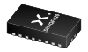
Nexperia B.V. 1-to-4 fan-out buffer 74AVC1T1022DPJ

Description
The 74AVC1T1022 is a translating 1-to-4 fan-out buffer suitable for use in clock distribution. It has dual supplies (VCC(A) and VCC(B)) for voltage translation. It also has a data input (A), four data outputs (1Yn and 2Yn) and an output enable input (OE). VCC(A) and VCC(B) can be independently supplied at any voltage between 0.8 V and 3.6 V. It makes the device suitable for low voltage translation between any of the following voltages: 0.8 V, 1.2 V, 1.5 V, 1.8 V, 2.5 V and 3.3 V. The levels of A, OEand 1Yn are referenced to VCC(A), outputs 2Yn are referenced to VCC(B). This supply configuration ensures that two of the fanned out signals can be used in level shifting. A HIGH on OEcauses all outputs to be pulled LOW via pull-down resistors, a LOW on OEdisconnects the pull-down resistors and enables all outputs. Schmitt trigger action at all inputs makes the circuit tolerant for slower input rise and fall time. The IOFF circuitry disables the output, preventing any damaging backflow current through the device when it is powered down. Features and benefits Wide supply voltage range: VCC(A): 0.8 V to 3.6 V VCC(B): 0.8 V to 3.6 V Complies with JEDEC standards: JESD8-12 (0.8 V to 1.3 V) JESD8-11 (0.9 V to 1.65 V) JESD8-7 (1.2 V to 1.95 V) JESD8-5 (1.8 V to 2.7 V) JESD8-B (2.7 V to 3.6 V) Maximum data rates: 380 Mbit/s (≥ 1.8 V to 3.3 V translation) 200 Mbit/s (≥ 1.1 V to 3.3 V translation) 200 Mbit/s (≥ 1.1 V to 2.5 V translation) 200 Mbit/s (≥ 1.1 V to 1.8 V translation) 150 Mbit/s (≥ 1.1 V to 1.5 V translation) 100 Mbit/s (≥ 1.1 V to 1.2 V translation) Latch-up performance exceeds 100 mA per JESD 78 Class II Inputs accept voltages up to 3.6 V ESD protection: HBM: ANSI/ESDA/JEDEC JS-001 class 3B exceeds 8000 V CDM: ANSI/ESDA/JEDEC JS-002 class C3 exceeds 1000 V Specified from -40 °C to +85 °C and -40 °C to +125 °C
Request a Quote Datasheet
Description
The 74AVC1T1022 is a translating 1-to-4 fan-out buffer suitable for use in clock distribution. It has dual supplies (VCC(A) and VCC(B)) for voltage translation. It also has a data input (A), four data outputs (1Yn and 2Yn) and an output enable input (OE). VCC(A) and VCC(B) can be independently supplied at any voltage between 0.8 V and 3.6 V. It makes the device suitable for low voltage translation between any of the following voltages: 0.8 V, 1.2 V, 1.5 V, 1.8 V, 2.5 V and 3.3 V. The levels of A, OEand 1Yn are referenced to VCC(A), outputs 2Yn are referenced to VCC(B). This supply configuration ensures that two of the fanned out signals can be used in level shifting. A HIGH on OEcauses all outputs to be pulled LOW via pull-down resistors, a LOW on OEdisconnects the pull-down resistors and enables all outputs. Schmitt trigger action at all inputs makes the circuit tolerant for slower input rise and fall time. The IOFF circuitry disables the output, preventing any damaging backflow current through the device when it is powered down. Features and benefits Wide supply voltage range: VCC(A): 0.8 V to 3.6 V VCC(B): 0.8 V to 3.6 V Complies with JEDEC standards: JESD8-12 (0.8 V to 1.3 V) JESD8-11 (0.9 V to 1.65 V) JESD8-7 (1.2 V to 1.95 V) JESD8-5 (1.8 V to 2.7 V) JESD8-B (2.7 V to 3.6 V) Maximum data rates: 380 Mbit/s (≥ 1.8 V to 3.3 V translation) 200 Mbit/s (≥ 1.1 V to 3.3 V translation) 200 Mbit/s (≥ 1.1 V to 2.5 V translation) 200 Mbit/s (≥ 1.1 V to 1.8 V translation) 150 Mbit/s (≥ 1.1 V to 1.5 V translation) 100 Mbit/s (≥ 1.1 V to 1.2 V translation) Latch-up performance exceeds 100 mA per JESD 78 Class II Inputs accept voltages up to 3.6 V ESD protection: HBM: ANSI/ESDA/JEDEC JS-001 class 3B exceeds 8000 V CDM: ANSI/ESDA/JEDEC JS-002 class C3 exceeds 1000 V Specified from -40 °C to +85 °C and -40 °C to +125 °C
Request a Quote Datasheet

Suppliers

Company
Product
Description
Supplier Links
1-to-4 fan-out buffer - 74AVC1T1022DPJ - Nexperia B.V.
Nijmegen, Netherlands
1-to-4 fan-out buffer
74AVC1T1022DPJ
1-to-4 fan-out buffer 74AVC1T1022DPJ
The 74AVC1T1022 is a translating 1-to-4 fan-out buffer suitable for use in clock distribution. It has dual supplies (VCC(A) and VCC(B)) for voltage translation. It also has a data input (A), four data outputs (1Yn and 2Yn) and an output enable input (OE). VCC(A) and VCC(B) can be independently supplied at any voltage between 0.8 V and 3.6 V. It makes the device suitable for low voltage translation between any of the following voltages: 0.8 V, 1.2 V, 1.5 V, 1.8 V, 2.5 V and 3.3 V. The levels of A, OEand 1Yn are referenced to VCC(A), outputs 2Yn are referenced to VCC(B). This supply configuration ensures that two of the fanned out signals can be used in level shifting. A HIGH on OEcauses all outputs to be pulled LOW via pull-down resistors, a LOW on OEdisconnects the pull-down resistors and enables all outputs. Schmitt trigger action at all inputs makes the circuit tolerant for slower input rise and fall time. The IOFF circuitry disables the output, preventing any damaging backflow current through the device when it is powered down. Features and benefits Wide supply voltage range: VCC(A): 0.8 V to 3.6 V VCC(B): 0.8 V to 3.6 V Complies with JEDEC standards: JESD8-12 (0.8 V to 1.3 V) JESD8-11 (0.9 V to 1.65 V) JESD8-7 (1.2 V to 1.95 V) JESD8-5 (1.8 V to 2.7 V) JESD8-B (2.7 V to 3.6 V) Maximum data rates: 380 Mbit/s (≥ 1.8 V to 3.3 V translation) 200 Mbit/s (≥ 1.1 V to 3.3 V translation) 200 Mbit/s (≥ 1.1 V to 2.5 V translation) 200 Mbit/s (≥ 1.1 V to 1.8 V translation) 150 Mbit/s (≥ 1.1 V to 1.5 V translation) 100 Mbit/s (≥ 1.1 V to 1.2 V translation) Latch-up performance exceeds 100 mA per JESD 78 Class II Inputs accept voltages up to 3.6 V ESD protection: HBM: ANSI/ESDA/JEDEC JS-001 class 3B exceeds 8000 V CDM: ANSI/ESDA/JEDEC JS-002 class C3 exceeds 1000 V Specified from -40 °C to +85 °C and -40 °C to +125 °C

The 74AVC1T1022 is a translating 1-to-4 fan-out buffer suitable for use in clock distribution. It has dual supplies (VCC(A) and VCC(B)) for voltage translation. It also has a data input (A), four data outputs (1Yn and 2Yn) and an output enable input (OE). VCC(A) and VCC(B) can be independently supplied at any voltage between 0.8 V and 3.6 V. It makes the device suitable for low voltage translation between any of the following voltages: 0.8 V, 1.2 V, 1.5 V, 1.8 V, 2.5 V and 3.3 V. The levels of A, OEand 1Yn are referenced to VCC(A), outputs 2Yn are referenced to VCC(B). This supply configuration ensures that two of the fanned out signals can be used in level shifting. A HIGH on OEcauses all outputs to be pulled LOW via pull-down resistors, a LOW on OEdisconnects the pull-down resistors and enables all outputs.

Schmitt trigger action at all inputs makes the circuit tolerant for slower input rise and fall time.

The IOFF circuitry disables the output, preventing any damaging backflow current through the device when it is powered down.

Features and benefits

  • Wide supply voltage range:
    • VCC(A): 0.8 V to 3.6 V
    • VCC(B): 0.8 V to 3.6 V
  • Complies with JEDEC standards:
    • JESD8-12 (0.8 V to 1.3 V)
    • JESD8-11 (0.9 V to 1.65 V)
    • JESD8-7 (1.2 V to 1.95 V)
    • JESD8-5 (1.8 V to 2.7 V)
    • JESD8-B (2.7 V to 3.6 V)
  • Maximum data rates:
    • 380 Mbit/s (≥ 1.8 V to 3.3 V translation)
    • 200 Mbit/s (≥ 1.1 V to 3.3 V translation)
    • 200 Mbit/s (≥ 1.1 V to 2.5 V translation)
    • 200 Mbit/s (≥ 1.1 V to 1.8 V translation)
    • 150 Mbit/s (≥ 1.1 V to 1.5 V translation)
    • 100 Mbit/s (≥ 1.1 V to 1.2 V translation)
  • Latch-up performance exceeds 100 mA per JESD 78 Class II
  • Inputs accept voltages up to 3.6 V
  • ESD protection:
    • HBM: ANSI/ESDA/JEDEC JS-001 class 3B exceeds 8000 V
    • CDM: ANSI/ESDA/JEDEC JS-002 class C3 exceeds 1000 V
  • Specified from -40 °C to +85 °C and -40 °C to +125 °C
Supplier's Site Datasheet

Technical Specifications

  Nexperia B.V.
Product Category IC Interfaces
Product Number 74AVC1T1022DPJ
Product Name 1-to-4 fan-out buffer
Device Type Buffer
Unlock Full Specs
to access all available technical data

Similar Products

Single Schmitt trigger buffer - 74AHC1G17GW-Q100H - Nexperia B.V.
Specs
Device Type Buffer
Features RoHS
Supply Voltage Other; +7.0
View Details
Octal buffer/line driver; 3-state - 74AHC244BQ-Q100,11 - Nexperia B.V.
Specs
Device Type Buffer
Features RoHS
Supply Voltage Other; +7.0
View Details
Octal buffer/line driver; 3-state - 74AHCT244BQ,115 - Nexperia B.V.
Specs
Device Type Buffer
Features RoHS
Supply Voltage Other; +7.0
View Details
3 suppliers
Octal buffer/line driver; 3-state - 74AHCT244BQ/GX - Nexperia B.V.
Specs
Device Type Buffer
Features RoHS
Supply Voltage Other; +7.0
View Details