Nexperia B.V. Low-power dual 2-input NAND gate 74AUP2G00DC/GH

Description
The 74AUP2G00 provides dual 2-input NAND function. Schmitt trigger action at all inputs makes the circuit tolerant to slower input rise and fall times across the entire VCC range from 0.8 V to 3.6 V. This device ensures a very low static and dynamic power consumption across the entire VCC range from 0.8 V to 3.6 V. This device is fully specified for partial power-down applications using IOFF. The IOFF circuitry disables the output, preventing a damaging backflow current through the device when it is powered down. Features and benefits Wide supply voltage range from 0.8 V to 3.6 V High noise immunity Complies with JEDEC standards: JESD8-12 (0.8 V to 1.3 V) JESD8-11 (0.9 V to 1.65 V) JESD8-7 (1.2 V to 1.95 V) JESD8-5 (1.8 V to 2.7 V) JESD8-B (2.7 V to 3.6 V) Low static power consumption; ICC = 0.9 μA (maximum) Latch-up performance exceeds 100 mA per JESD78 Class II Inputs accept voltages up to 3.6 V Low noise overshoot and undershoot < 10 % of VCC IOFF circuitry provides partial power-down mode operation ESD protection: HBM: ANSI/ESDA/JEDEC JS-001 class 3A exceeds 5000 V CDM: ANSI/ESDA/JEDEC JS-002 class C3 exceeds 1000 V Multiple package options Specified from -40 °C to +85 °C and -40 °C to +125 °C
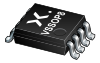
Request a Quote Datasheet
Description
The 74AUP2G00 provides dual 2-input NAND function. Schmitt trigger action at all inputs makes the circuit tolerant to slower input rise and fall times across the entire VCC range from 0.8 V to 3.6 V. This device ensures a very low static and dynamic power consumption across the entire VCC range from 0.8 V to 3.6 V. This device is fully specified for partial power-down applications using IOFF. The IOFF circuitry disables the output, preventing a damaging backflow current through the device when it is powered down. Features and benefits Wide supply voltage range from 0.8 V to 3.6 V High noise immunity Complies with JEDEC standards: JESD8-12 (0.8 V to 1.3 V) JESD8-11 (0.9 V to 1.65 V) JESD8-7 (1.2 V to 1.95 V) JESD8-5 (1.8 V to 2.7 V) JESD8-B (2.7 V to 3.6 V) Low static power consumption; ICC = 0.9 μA (maximum) Latch-up performance exceeds 100 mA per JESD78 Class II Inputs accept voltages up to 3.6 V Low noise overshoot and undershoot < 10 % of VCC IOFF circuitry provides partial power-down mode operation ESD protection: HBM: ANSI/ESDA/JEDEC JS-001 class 3A exceeds 5000 V CDM: ANSI/ESDA/JEDEC JS-002 class C3 exceeds 1000 V Multiple package options Specified from -40 °C to +85 °C and -40 °C to +125 °C
Request a Quote Datasheet

Suppliers

Company
Product
Description
Supplier Links
Low-power dual 2-input NAND gate - 74AUP2G00DC/GH - Nexperia B.V.
Nijmegen, Netherlands
Low-power dual 2-input NAND gate
74AUP2G00DC/GH
Low-power dual 2-input NAND gate 74AUP2G00DC/GH
The 74AUP2G00 provides dual 2-input NAND function. Schmitt trigger action at all inputs makes the circuit tolerant to slower input rise and fall times across the entire VCC range from 0.8 V to 3.6 V. This device ensures a very low static and dynamic power consumption across the entire VCC range from 0.8 V to 3.6 V. This device is fully specified for partial power-down applications using IOFF. The IOFF circuitry disables the output, preventing a damaging backflow current through the device when it is powered down. Features and benefits Wide supply voltage range from 0.8 V to 3.6 V High noise immunity Complies with JEDEC standards: JESD8-12 (0.8 V to 1.3 V) JESD8-11 (0.9 V to 1.65 V) JESD8-7 (1.2 V to 1.95 V) JESD8-5 (1.8 V to 2.7 V) JESD8-B (2.7 V to 3.6 V) Low static power consumption; ICC = 0.9 μA (maximum) Latch-up performance exceeds 100 mA per JESD78 Class II Inputs accept voltages up to 3.6 V Low noise overshoot and undershoot < 10 % of VCC IOFF circuitry provides partial power-down mode operation ESD protection: HBM: ANSI/ESDA/JEDEC JS-001 class 3A exceeds 5000 V CDM: ANSI/ESDA/JEDEC JS-002 class C3 exceeds 1000 V Multiple package options Specified from -40 °C to +85 °C and -40 °C to +125 °C
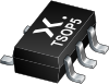
The 74AUP2G00 provides dual 2-input NAND function.

Schmitt trigger action at all inputs makes the circuit tolerant to slower input rise and fall times across the entire VCC range from 0.8 V to 3.6 V.

This device ensures a very low static and dynamic power consumption across the entire VCC range from 0.8 V to 3.6 V.

This device is fully specified for partial power-down applications using IOFF. The IOFF circuitry disables the output, preventing a damaging backflow current through the device when it is powered down.

Features and benefits

  • Wide supply voltage range from 0.8 V to 3.6 V
  • High noise immunity
  • Complies with JEDEC standards:
    • JESD8-12 (0.8 V to 1.3 V)
    • JESD8-11 (0.9 V to 1.65 V)
    • JESD8-7 (1.2 V to 1.95 V)
    • JESD8-5 (1.8 V to 2.7 V)
    • JESD8-B (2.7 V to 3.6 V)
  • Low static power consumption; ICC = 0.9 μA (maximum)
  • Latch-up performance exceeds 100 mA per JESD78 Class II
  • Inputs accept voltages up to 3.6 V
  • Low noise overshoot and undershoot < 10 % of VCC
  • IOFF circuitry provides partial power-down mode operation
  • ESD protection:
    • HBM: ANSI/ESDA/JEDEC JS-001 class 3A exceeds 5000 V
    • CDM: ANSI/ESDA/JEDEC JS-002 class C3 exceeds 1000 V
  • Multiple package options
  • Specified from -40 °C to +85 °C and -40 °C to +125 °C
Supplier's Site Datasheet

Technical Specifications

  Nexperia B.V.
Product Category Logic Gates
Product Number 74AUP2G00DC/GH
Product Name Low-power dual 2-input NAND gate
Gate Type NAND
Unlock Full Specs
to access all available technical data

Similar Products

2-input NOR gate - 74AHC1G02GV-Q100H - Nexperia B.V.
Specs
Gate Type NOR
Supply Voltage +7.0
IC Package Type Other; SOT753 SOT753
View Details
6 suppliers
TSSOP Logic IC - 705-74AHC1G04GW,125 - ERSAELECTRONICS PTE. LTD.
Specs
Gate Type NOT
Logic Family AHC/VHC/H/U/V
Inputs 1
View Details
8 suppliers
Quad 2-input OR gate - 74AHC32D,118 - Nexperia B.V.
Specs
Gate Type OR
Supply Voltage +7.0
IC Package Type Other; SOT108-1 SOT108-1
View Details
9 suppliers
Specs
Logic Family AHC/VHC/H/U/V
Operating Temperature -40 C (-40 F)
Pin Count 20
View Details