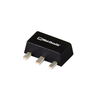
Mini-Circuits SMT MMIC, Medium Power, Linear, HBT, Low Phase Noise Amplifier, DC to 6000 MHz, 50Ω, SOT-89 Style Package GVA-81+

Description
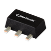
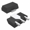
GVA-81+ (RoHS compliant) is a wideband amplifier offering high dynamic range. It has repeatable performance from lot to lot and is enclosed in a SOT-89 package. It uses patented Transient Protected Darlington configuration and is fabricated using InGaP HBT technology. SIMPLIFIED SCHEMATIC AND PIN DESCRIPTION RF-OUT and DC-IN RF IN 3 RF-OUT & DC-IN 4 2 GROUND 1 RF-IN GROUND Pin Function Description Number RF IN 1 RF input pin. This pin requires the use of an external DC blocking capacitor chosen for the frequency of operation. RF-OUT RF output and bias pin. DC voltage is present on this pin; therefore a DC blocking capacitor is necessary for proper operation. An RF choke 3 and DC-IN is needed to feed DC bias without loss of RF signal due to the bias connection, as shown in “Recommended Application Circuit”, Fig. 2 Connections to ground. Use via holes as shown in “Suggested Layout for PCB Design” to reduce ground path inductance for best GND 2,4 performance. A. Suitability for model replacement within a particular system must be determined by and is solely the responsibility of the customer based on, among other things, electrical performance criteria, stimulus conditions, application, compatibility with other components and environmental conditions and stresses. B. The RFMD SBB4089Z part number is used for identification and comparison purposes only. REV. C ECO-010563 GVA-81+ 240207 www.minicircuits.com P.O. Box 350166, Brooklyn, NY 11235-0003 (718) 934-4500 sales@minicircuits.c om PAGE 1 OF 1 5 VOLT-SURFACE MOUNT Monolithic Amplifier GVA-81+
Request a Quote Datasheet
Description
GVA-81+ (RoHS compliant) is a wideband amplifier offering high dynamic range. It has repeatable performance from lot to lot and is enclosed in a SOT-89 package. It uses patented Transient Protected Darlington configuration and is fabricated using InGaP HBT technology. SIMPLIFIED SCHEMATIC AND PIN DESCRIPTION RF-OUT and DC-IN RF IN 3 RF-OUT & DC-IN 4 2 GROUND 1 RF-IN GROUND Pin Function Description Number RF IN 1 RF input pin. This pin requires the use of an external DC blocking capacitor chosen for the frequency of operation. RF-OUT RF output and bias pin. DC voltage is present on this pin; therefore a DC blocking capacitor is necessary for proper operation. An RF choke 3 and DC-IN is needed to feed DC bias without loss of RF signal due to the bias connection, as shown in “Recommended Application Circuit”, Fig. 2 Connections to ground. Use via holes as shown in “Suggested Layout for PCB Design” to reduce ground path inductance for best GND 2,4 performance. A. Suitability for model replacement within a particular system must be determined by and is solely the responsibility of the customer based on, among other things, electrical performance criteria, stimulus conditions, application, compatibility with other components and environmental conditions and stresses. B. The RFMD SBB4089Z part number is used for identification and comparison purposes only. REV. C ECO-010563 GVA-81+ 240207 www.minicircuits.com P.O. Box 350166, Brooklyn, NY 11235-0003 (718) 934-4500 sales@minicircuits.c om PAGE 1 OF 1 5 VOLT-SURFACE MOUNT Monolithic Amplifier GVA-81+
Request a Quote Datasheet

Suppliers

Company
Product
Description
Supplier Links
SMT MMIC, Medium Power, Linear, HBT, Low Phase Noise Amplifier, DC to 6000 MHz, 50Ω, SOT-89 Style Package - GVA-81+ - Mini-Circuits
Brooklyn, NY, United States
SMT MMIC, Medium Power, Linear, HBT, Low Phase Noise Amplifier, DC to 6000 MHz, 50Ω, SOT-89 Style Package
GVA-81+
SMT MMIC, Medium Power, Linear, HBT, Low Phase Noise Amplifier, DC to 6000 MHz, 50Ω, SOT-89 Style Package GVA-81+
GVA-81+ (RoHS compliant) is a wideband amplifier offering high dynamic range. It has repeatable performance from lot to lot and is enclosed in a SOT-89 package. It uses patented Transient Protected Darlington configuration and is fabricated using InGaP HBT technology. SIMPLIFIED SCHEMATIC AND PIN DESCRIPTION RF-OUT and DC-IN RF IN 3 RF-OUT & DC-IN 4 2 GROUND 1 RF-IN GROUND Pin Function Description Number RF IN 1 RF input pin. This pin requires the use of an external DC blocking capacitor chosen for the frequency of operation. RF-OUT RF output and bias pin. DC voltage is present on this pin; therefore a DC blocking capacitor is necessary for proper operation. An RF choke 3 and DC-IN is needed to feed DC bias without loss of RF signal due to the bias connection, as shown in “Recommended Application Circuit”, Fig. 2 Connections to ground. Use via holes as shown in “Suggested Layout for PCB Design” to reduce ground path inductance for best GND 2,4 performance. A. Suitability for model replacement within a particular system must be determined by and is solely the responsibility of the customer based on, among other things, electrical performance criteria, stimulus conditions, application, compatibility with other components and environmental conditions and stresses. B. The RFMD SBB4089Z part number is used for identification and comparison purposes only. REV. C ECO-010563 GVA-81+ 240207 www.minicircuits.com P.O. Box 350166, Brooklyn, NY 11235-0003 (718) 934-4500 sales@minicircuits.c om PAGE 1 OF 1 5 VOLT-SURFACE MOUNT Monolithic Amplifier GVA-81+

GVA-81+ (RoHS compliant) is a wideband amplifier offering high dynamic range. It has repeatable performance from lot to lot and is enclosed in a SOT-89 package. It uses patented Transient Protected Darlington configuration and is fabricated using InGaP HBT technology. SIMPLIFIED SCHEMATIC AND PIN DESCRIPTION RF-OUT and DC-IN RF IN 3 RF-OUT & DC-IN 4 2 GROUND 1 RF-IN GROUND Pin Function Description Number RF IN 1 RF input pin. This pin requires the use of an external DC blocking capacitor chosen for the frequency of operation. RF-OUT RF output and bias pin. DC voltage is present on this pin; therefore a DC blocking capacitor is necessary for proper operation. An RF choke 3 and DC-IN is needed to feed DC bias without loss of RF signal due to the bias connection, as shown in “Recommended Application Circuit”, Fig. 2 Connections to ground. Use via holes as shown in “Suggested Layout for PCB Design” to reduce ground path inductance for best GND 2,4 performance. A. Suitability for model replacement within a particular system must be determined by and is solely the responsibility of the customer based on, among other things, electrical performance criteria, stimulus conditions, application, compatibility with other components and environmental conditions and stresses. B. The RFMD SBB4089Z part number is used for identification and comparison purposes only. REV. C ECO-010563 GVA-81+ 240207 www.minicircuits.com P.O. Box 350166, Brooklyn, NY 11235-0003 (718) 934-4500 sales@minicircuits.com PAGE 1 OF 1 5 VOLT-SURFACE MOUNT Monolithic Amplifier GVA-81+

Supplier's Site Datasheet
Laguna Hills, CA, United States
RF Amplifiers - GVA-81+
718443-GVA-81+
RF Amplifiers - GVA-81+ 718443-GVA-81+
Manufacturer: Mini-Circuits Win Source Part Number: 718443-GVA-81+ Manufacturer Homepage: www.minicircuits.com Reference Date Code: 1605+ Popularity: Medium Fake Threat In the Open Market: 62 pct. Supply and Demand Status: Limited

Manufacturer: Mini-Circuits
Win Source Part Number: 718443-GVA-81+
Manufacturer Homepage: www.minicircuits.com
Reference Date Code: 1605+
Popularity: Medium
Fake Threat In the Open Market: 62 pct.
Supply and Demand Status: Limited

Buy Now
RF Amplifiers - 3157-GVA-81+TR-ND - DigiKey
Thief River Falls, MN, United States
RF Amplifiers
3157-GVA-81+TR-ND
RF Amplifiers 3157-GVA-81+TR-ND
RF Amplifier IC CATV, DBS, LTE, MMDS, Wireless LAN 0Hz ~ 6GHz SOT-89

RF Amplifier IC CATV, DBS, LTE, MMDS, Wireless LAN 0Hz ~ 6GHz SOT-89

Buy Now Datasheet
RF Amplifiers - 3157-GVA-81+DKR-ND - DigiKey
Thief River Falls, MN, United States
RF Amplifiers
3157-GVA-81+DKR-ND
RF Amplifiers 3157-GVA-81+DKR-ND
RF Amplifier IC CATV, DBS, LTE, MMDS, Wireless LAN 0Hz ~ 6GHz SOT-89

RF Amplifier IC CATV, DBS, LTE, MMDS, Wireless LAN 0Hz ~ 6GHz SOT-89

Buy Now Datasheet
RF Amplifiers - 3157-GVA-81+CT-ND - DigiKey
Thief River Falls, MN, United States
RF Amplifiers
3157-GVA-81+CT-ND
RF Amplifiers 3157-GVA-81+CT-ND
RF Amplifier IC CATV, DBS, LTE, MMDS, Wireless LAN 0Hz ~ 6GHz SOT-89

RF Amplifier IC CATV, DBS, LTE, MMDS, Wireless LAN 0Hz ~ 6GHz SOT-89

Buy Now Datasheet
RF and Wireless - RF Amplifiers - GVA-81+ - Shenzhen Shengyu Electronics Technology Limited
Futian, China
RF and Wireless - RF Amplifiers
GVA-81+
RF and Wireless - RF Amplifiers GVA-81+
IC RF AMP CATV 0HZ-6GHZ SOT89

IC RF AMP CATV 0HZ-6GHZ SOT89

Supplier's Site

Technical Specifications

  Mini-Circuits Win Source Electronics DigiKey Shenzhen Shengyu Electronics Technology Limited
Product Category RF Amplifiers RF Amplifiers RF Amplifiers RF Amplifiers
Product Number GVA-81+ 718443-GVA-81+ 3157-GVA-81+TR-ND GVA-81+
Product Name SMT MMIC, Medium Power, Linear, HBT, Low Phase Noise Amplifier, DC to 6000 MHz, 50Ω, SOT-89 Style Package RF Amplifiers - GVA-81+ RF Amplifiers RF and Wireless - RF Amplifiers
Amplifier Type Power Amplifier Low Noise Amplifier; Power Amplifier
RoHS Compliant RoHS
Frequency Range 6000 MHz 0.0 to 6000 MHz 0.0 to 6000 MHz
Minimum Gain 5.00E-4 dB 8.1 dB ? to 8.1 dB
Maximum Gain 11.5 dB 8.1 dB 8.1 dB
Unlock Full Specs
to access all available technical data

Similar Products

Connectorized SMA, Linear, Gain Block Amplifier, 500 MHz to 2500 MHz, 50Ω - ZFL-2500B+ - Mini-Circuits
Specs
Operating Temperature -20 to 65 C (-4 to 149 F)
Package Type Connectorized
Connectors SMA
View Details
Specs
Applications RF Microwave
View Details
Connectorized SMA, Low Noise, Linear Amplifier, 0.1 MHz to 1000 MHz, 50Ω - ZFL-1000LNB+ - Mini-Circuits
Specs
Amplifier Type Low Noise Amplifier
Operating Temperature -20 to 71 C (-4 to 160 F)
Frequency Range 0.1000 to 1000 MHz
View Details
3 suppliers
SMT, Low Noise, Medium Power, Linear, pHEMT Amplifier Module, 1710 MHz to 2400 MHz, 50Ω, 15x10 mm Package - TAMP-242LN+ - Mini-Circuits
Specs
Amplifier Type Low Noise Amplifier; Power Amplifier
RoHS Compliant RoHS
Operating Temperature -40 to 85 C (-40 to 185 F)
View Details