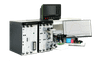
Automated Thickness measurement system
IR interferometry probe technology. Single or dual probes.
Manual Loading
0.5um accuracy. 0.1um resolution
Wafer 4" to 12" (100 to 300mm) round or square
Thickness range: 20um to 1mm
Flexible recipe generation
2D & 3D mapping capability
SECS/GEM communication
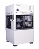
Options
Extended warp/bow range up to 5000um
Wafer prealigner
Samples with special shape (square, rectangle, round)
Applications
Thickness and shape measurement of wafers with backgrinding tape wafer on sawframe, dies on tape, wafer on bumps, SOI, multiple layers, bonded wafers, thickness of Si, plastic, glass, adhesive layers.
Automated Thickness measurement system
IR interferometry probe technology. Single or dual probes.
Manual Loading
- 0.5um accuracy. 0.1um resolution
- Wafer 4" to 12" (100 to 300mm) round or square
- Thickness range: 20um to 1mm
- Flexible recipe generation
- 2D & 3D mapping capability
- SECS/GEM communication
Options
- Extended warp/bow range up to 5000um
- Wafer prealigner
- Samples with special shape (square, rectangle, round)
Applications
Thickness and shape measurement of wafers with backgrinding tape wafer on sawframe, dies on tape, wafer on bumps, SOI,
multiple layers, bonded wafers, thickness of Si, plastic, glass,
adhesive layers.