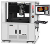
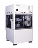
Benchtop automated thickness measurement system with X-Y stage on air bearing for wafers up to 8” round and for square wafers up to 156mmx156mm.
Solar Wafers QA and QC, Cost effective, compact metrology tool for R&D labs for all type of wafers and surfaces.
| MicroSense, LLC | |
|---|---|
| Product Category | Wafer and Thin Film Instrumentation |
| Product Number | UltraMap-200B |
| Product Name | SigmaTech Wafer Metrology Systems |
| Form Factor | Monitor or instrument |
| Mounting / Loading | Manual loading |
| Technology | Optical / Imaging |