Microchip Technology, Inc. N/P-Channel Enhancement-Mode Dual MOSFET TC6320

Description
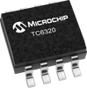
TC6320 consists of high voltage, low threshold N-channel and P-channel MOSFETs in 8-Lead SOIC and DFN packages. Both MOSFETs have integrated GATE-to-SOURCE resistors and GATE-to-SOURCE Zener diode clamps which are desired for high voltage pulser applications. It is a complimentary, high-speed, high voltage, GATE-clamped N- and P-channel MOSFET pair, which utilizes an advanced vertical DMOS structure and well-proven silicon-gate manufacturing process. This combination produces a device with the power handling capabilities of bipolar transistors and with the high input impedance and positive temperature coefficient inherent in MOS devices. Characteristic of all MOS structures, this device is free from thermal runaway and thermally induced secondary breakdown. Vertical DMOS FETs are ideally suited to a wide range of switching and amplifying applications where very low threshold voltage, high breakdown voltage, high input impedance, low input capacitance, and fast switching speeds are desired. Additional Features Integrated GATE-to-SOURCE resistor Integrated GATE-to-SOURCE Zener diode Low threshold Low on-resistance Low input capacitance Fast switching speeds Free from secondary breakdown Low input and output leakage Independent, electrically isolated N- and P-channels
Datasheet
Description
TC6320 consists of high voltage, low threshold N-channel and P-channel MOSFETs in 8-Lead SOIC and DFN packages. Both MOSFETs have integrated GATE-to-SOURCE resistors and GATE-to-SOURCE Zener diode clamps which are desired for high voltage pulser applications. It is a complimentary, high-speed, high voltage, GATE-clamped N- and P-channel MOSFET pair, which utilizes an advanced vertical DMOS structure and well-proven silicon-gate manufacturing process. This combination produces a device with the power handling capabilities of bipolar transistors and with the high input impedance and positive temperature coefficient inherent in MOS devices. Characteristic of all MOS structures, this device is free from thermal runaway and thermally induced secondary breakdown. Vertical DMOS FETs are ideally suited to a wide range of switching and amplifying applications where very low threshold voltage, high breakdown voltage, high input impedance, low input capacitance, and fast switching speeds are desired. Additional Features Integrated GATE-to-SOURCE resistor Integrated GATE-to-SOURCE Zener diode Low threshold Low on-resistance Low input capacitance Fast switching speeds Free from secondary breakdown Low input and output leakage Independent, electrically isolated N- and P-channels
Datasheet

Suppliers

Company
Product
Description
Supplier Links
N/P-Channel Enhancement-Mode Dual MOSFET - TC6320 - Microchip Technology, Inc.
Chandler, AZ, United States
N/P-Channel Enhancement-Mode Dual MOSFET
TC6320
N/P-Channel Enhancement-Mode Dual MOSFET TC6320
TC6320 consists of high voltage, low threshold N-channel and P-channel MOSFETs in 8-Lead SOIC and DFN packages. Both MOSFETs have integrated GATE-to-SOURCE resistors and GATE-to-SOURCE Zener diode clamps which are desired for high voltage pulser applications. It is a complimentary, high-speed, high voltage, GATE-clamped N- and P-channel MOSFET pair, which utilizes an advanced vertical DMOS structure and well-proven silicon-gate manufacturing process. This combination produces a device with the power handling capabilities of bipolar transistors and with the high input impedance and positive temperature coefficient inherent in MOS devices. Characteristic of all MOS structures, this device is free from thermal runaway and thermally induced secondary breakdown. Vertical DMOS FETs are ideally suited to a wide range of switching and amplifying applications where very low threshold voltage, high breakdown voltage, high input impedance, low input capacitance, and fast switching speeds are desired. Additional Features Integrated GATE-to-SOURCE resistor Integrated GATE-to-SOURCE Zener diode Low threshold Low on-resistance Low input capacitance Fast switching speeds Free from secondary breakdown Low input and output leakage Independent, electrically isolated N- and P-channels
TC6320 consists of high voltage, low threshold N-channel and P-channel MOSFETs in 8-Lead SOIC and DFN packages. Both MOSFETs have integrated GATE-to-SOURCE resistors and GATE-to-SOURCE Zener diode clamps which are desired for high voltage pulser applications. It is a complimentary, high-speed, high voltage, GATE-clamped N- and P-channel MOSFET pair, which utilizes an advanced vertical DMOS structure and well-proven silicon-gate manufacturing process. This combination produces a device with the power handling capabilities of bipolar transistors and with the high input impedance and positive temperature coefficient inherent in MOS devices. Characteristic of all MOS structures, this device is free from thermal runaway and thermally induced secondary breakdown. Vertical DMOS FETs are ideally suited to a wide range of switching and amplifying applications where very low threshold voltage, high breakdown voltage, high input impedance, low input capacitance, and fast switching speeds are desired.

Additional Features

    • Integrated GATE-to-SOURCE resistor
    • Integrated GATE-to-SOURCE Zener diode
    • Low threshold
    • Low on-resistance
    • Low input capacitance
    • Fast switching speeds
    • Free from secondary breakdown
    • Low input and output leakage
    • Independent, electrically isolated N- and P-channels

Supplier's Site Datasheet

Technical Specifications

  Microchip Technology, Inc.
Product Category Metal-Oxide Semiconductor FET (MOSFET)
Product Number TC6320
Product Name N/P-Channel Enhancement-Mode Dual MOSFET
Polarity P-Channel
Unlock Full Specs
to access all available technical data