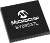
The SY89537L integrated programmable clock synthesizer and fanout is part of a precision PLL-based clock generation family optimized for enterprise switch, router, and multiprocessor server applications. This family is ideal for generating internal system timing requirements up to 700MHz for multiple ASICs, FPGAs, and NPUs. These devices integrate the following blocks into a single monolithic IC: PLL (Phase-Lock-Loop) based synthesizer Fanout buffers Clock generator (dividers) Logic translation (LVPECL, LVDS) Five independently programmable output banksThis level of integration minimizes additive jitter and part-to-part skew associated with discrete alternatives, resulting in superior system-level timing with reduced board space and power. For applications that require a zero-delay function, see the SY89538L.
Additional Features
Integrated programmable synthesizer with multiple output dividers, fanout buffers, and clock drivers
Direct interface to crystal: 14MHz to 18MHz Input MUX accepts a reference and a crystal (XTAL) source
Ideal for reference backup clock source or system test frequency source
Patent-pending unique input MUX isolates XTAL and reference inputs minimizes crosstalk
Guaranteed AC performance:
87.15MHz to 700MHz output frequency range (with RFCK at 16.6MHz )
<100psPP total jitter
<7psRMS cycle-to-cycle jitter
<8psPP deterministic jitter
<0.7psRMS crosstalk induced jitter
<50ps bank-to-bank skew
Output bank synchronization control pin
LVPECL and LVDS outputs
TTL/CMOS compatible control logic
Five independently programmable output frequency banks:
Four differential LVPECL output banks
One differential LVDS output bank with 3 output pairs
Separate output enable for each bank
3.3V ±10% power supply (2.5V output capable)
Guaranteed over the industrial temperature range (-40°C to +85°C)
Available in 44-pin (7mm x 7mm) MLF® package
The SY89537L integrated programmable clock synthesizer and fanout is part of a precision PLL-based clock generation family optimized for enterprise switch, router, and multiprocessor server applications. This family is ideal for generating internal system timing requirements up to 700MHz for multiple ASICs, FPGAs, and NPUs. These devices integrate the following blocks into a single monolithic IC:
PLL (Phase-Lock-Loop) based synthesizer
Fanout buffers
Clock generator (dividers)
Logic translation (LVPECL, LVDS)
Five independently programmable output banksThis level of integration minimizes additive jitter and part-to-part skew associated with discrete alternatives, resulting in superior system-level timing with reduced board space and power. For applications that require a zero-delay function, see the SY89538L.
Additional Features
- Integrated programmable synthesizer with multiple output dividers, fanout buffers, and clock drivers
- Direct interface to crystal: 14MHz to 18MHz Input MUX accepts a reference and a crystal (XTAL) source
- Ideal for reference backup clock source or system test frequency source
- Patent-pending unique input MUX isolates XTAL and reference inputs minimizes crosstalk
- Guaranteed AC performance:
- 87.15MHz to 700MHz output frequency range (with RFCK at 16.6MHz )
- <100psPP total jitter
- <7psRMS cycle-to-cycle jitter
- <8psPP deterministic jitter
- <0.7psRMS crosstalk induced jitter
- <50ps bank-to-bank skew
- Output bank synchronization control pin
- LVPECL and LVDS outputs
- TTL/CMOS compatible control logic
- Five independently programmable output frequency banks:
- Four differential LVPECL output banks
- One differential LVDS output bank with 3 output pairs
- Separate output enable for each bank
- 3.3V ±10% power supply (2.5V output capable)
- Guaranteed over the industrial temperature range (-40°C to +85°C)
- Available in 44-pin (7mm x 7mm) MLF® package