Microchip Technology, Inc. SY89465U

Description
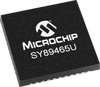
The SY89465U is a low-jitter, 1:10 LVDS fanout buffer with a 2:1 differential input multiplexer (MUX) optimized for redundant source switchover applications. Unlike standard multiplexers, the SY89465Us 2:1 Runt Pulse Eliminator (RPE) MUX prevents any short cycles or "runt" pulses during switchover. In addition, a unique Fail-Safe Input (FSI) protection prevents metastable conditions when the selected input clock fails to a DC voltage (voltage between the pins of the differential input drops below 100mV).The differential input includes Micrel's, 3-pin internal termination architecture that allows customers to interface to any differential signal (AC- or DC-coupled) as small as 100mV (200mVPP) without any level shifting or termination resistor networks in the signal path. The outputs are LVDS-compatible with fast rise/fall times guaranteed to be less than 220ps.The SY89465U operates from a 2.5V ±5% supply and is guaranteed over the full industrial temperature range of -40°C to +85°C. The SY89465U is part of Micrel's high-speed, Precision Edge® product line. Additional Features Selects between two sources, and provides 10 precision LVDS copies Guaranteed AC performance over temperature and supply voltage: Wide operating frequency: 1kHz to >1.5GHz <1200ps In-to-Out tpd <220ps tr/tf Unique, patent-pending input isolation design minimizes adjacent channel crosstalk Fail-Safe Input prevents oscillations Ultra-low jitter design: 183fsRMS phase jitter (typical) <0.7psRMS MUX crosstalk-induced jitter Unique patented input termination and VT pin accepts DC- and AC-coupled inputs (CML, PECL, LVDS) 325mV LVDS output swing 2.5V ±5% supply voltage −40°C to +85°C industrial temperature range Output enable Available in 44-pin (7mm x 7mm) QFN package
Datasheet
Description
The SY89465U is a low-jitter, 1:10 LVDS fanout buffer with a 2:1 differential input multiplexer (MUX) optimized for redundant source switchover applications. Unlike standard multiplexers, the SY89465Us 2:1 Runt Pulse Eliminator (RPE) MUX prevents any short cycles or "runt" pulses during switchover. In addition, a unique Fail-Safe Input (FSI) protection prevents metastable conditions when the selected input clock fails to a DC voltage (voltage between the pins of the differential input drops below 100mV).The differential input includes Micrel's, 3-pin internal termination architecture that allows customers to interface to any differential signal (AC- or DC-coupled) as small as 100mV (200mVPP) without any level shifting or termination resistor networks in the signal path. The outputs are LVDS-compatible with fast rise/fall times guaranteed to be less than 220ps.The SY89465U operates from a 2.5V ±5% supply and is guaranteed over the full industrial temperature range of -40°C to +85°C. The SY89465U is part of Micrel's high-speed, Precision Edge® product line. Additional Features Selects between two sources, and provides 10 precision LVDS copies Guaranteed AC performance over temperature and supply voltage: Wide operating frequency: 1kHz to >1.5GHz <1200ps In-to-Out tpd <220ps tr/tf Unique, patent-pending input isolation design minimizes adjacent channel crosstalk Fail-Safe Input prevents oscillations Ultra-low jitter design: 183fsRMS phase jitter (typical) <0.7psRMS MUX crosstalk-induced jitter Unique patented input termination and VT pin accepts DC- and AC-coupled inputs (CML, PECL, LVDS) 325mV LVDS output swing 2.5V ±5% supply voltage −40°C to +85°C industrial temperature range Output enable Available in 44-pin (7mm x 7mm) QFN package
Datasheet

Suppliers

Company
Product
Description
Supplier Links
 - SY89465U - Microchip Technology, Inc.
Chandler, AZ, United States
The SY89465U is a low-jitter, 1:10 LVDS fanout buffer with a 2:1 differential input multiplexer (MUX) optimized for redundant source switchover applications. Unlike standard multiplexers, the SY89465Us 2:1 Runt Pulse Eliminator (RPE) MUX prevents any short cycles or "runt" pulses during switchover. In addition, a unique Fail-Safe Input (FSI) protection prevents metastable conditions when the selected input clock fails to a DC voltage (voltage between the pins of the differential input drops below 100mV).The differential input includes Micrel's, 3-pin internal termination architecture that allows customers to interface to any differential signal (AC- or DC-coupled) as small as 100mV (200mVPP) without any level shifting or termination resistor networks in the signal path. The outputs are LVDS-compatible with fast rise/fall times guaranteed to be less than 220ps.The SY89465U operates from a 2.5V ±5% supply and is guaranteed over the full industrial temperature range of -40°C to +85°C. The SY89465U is part of Micrel's high-speed, Precision Edge® product line. Additional Features Selects between two sources, and provides 10 precision LVDS copies Guaranteed AC performance over temperature and supply voltage: Wide operating frequency: 1kHz to >1.5GHz <1200ps In-to-Out tpd <220ps tr/tf Unique, patent-pending input isolation design minimizes adjacent channel crosstalk Fail-Safe Input prevents oscillations Ultra-low jitter design: 183fsRMS phase jitter (typical) <0.7psRMS MUX crosstalk-induced jitter Unique patented input termination and VT pin accepts DC- and AC-coupled inputs (CML, PECL, LVDS) 325mV LVDS output swing 2.5V ±5% supply voltage −40°C to +85°C industrial temperature range Output enable Available in 44-pin (7mm x 7mm) QFN package

The SY89465U is a low-jitter, 1:10 LVDS fanout buffer with a 2:1 differential input multiplexer (MUX) optimized for redundant source switchover applications. Unlike standard multiplexers, the SY89465Us 2:1 Runt Pulse Eliminator (RPE) MUX prevents any short cycles or "runt" pulses during switchover. In addition, a unique Fail-Safe Input (FSI) protection prevents metastable conditions when the selected input clock fails to a DC voltage (voltage between the pins of the differential input drops below 100mV).The differential input includes Micrel's, 3-pin internal termination architecture that allows customers to interface to any differential signal (AC- or DC-coupled) as small as 100mV (200mVPP) without any level shifting or termination resistor networks in the signal path. The outputs are LVDS-compatible with fast rise/fall times guaranteed to be less than 220ps.The SY89465U operates from a 2.5V ±5% supply and is guaranteed over the full industrial temperature range of -40°C to +85°C. The SY89465U is part of Micrel's high-speed, Precision Edge® product line.

Additional Features

    • Selects between two sources, and provides 10 precision LVDS copies
    • Guaranteed AC performance over temperature and supply voltage:
      • Wide operating frequency: 1kHz to >1.5GHz
      • <1200ps In-to-Out tpd
      • <220ps tr/tf
    • Unique, patent-pending input isolation design minimizes adjacent channel crosstalk
    • Fail-Safe Input prevents oscillations
    • Ultra-low jitter design:
      • 183fsRMS phase jitter (typical)
      • <0.7psRMS MUX crosstalk-induced jitter
    • Unique patented input termination and VT pin accepts DC- and AC-coupled inputs (CML, PECL, LVDS)
    • 325mV LVDS output swing
    • 2.5V ±5% supply voltage
    • −40°C to +85°C industrial temperature range
    • Output enable
    • Available in 44-pin (7mm x 7mm) QFN package
Supplier's Site Datasheet

Technical Specifications

  Microchip Technology, Inc.
Product Category IC Analog Multiplexers
Product Number SY89465U
Package Type ['VQFN']
Unlock Full Specs
to access all available technical data

Similar Products

SN74CBTLV16292 Low-Voltage 12-Bit 1-Of-2 FET Multiplexer/Demultiplexer With Internal Pulldown Resistors - 74CBTLV16292VRG4 - Texas Instruments
Specs
Configuration 2 x 12 x SPDT (2 x 12 x 1:2)
Applications Catalog
Supply Voltage (VS) 2.3 to 3.6 volts
View Details
Signal Switches, Multiplexers, Decoders - 74HC151DB,118-ND - DigiKey
Specs
Operating Temperature -40 to 125 C (-40 to 257 F)
Package Type SSOP; "16-SSOP
View Details
2 suppliers
Multiplexer & Demultiplexer ICs - 1897126 - RS Components, Ltd.
Specs
Configuration Single SPST
Package Type SOT; SOT23; Sot-23
Number of Pins 5
View Details