The SST49LF080A flash memory device is designed to interface with the LPC bus for PC and Internet Appliance application in compliance with Intel Low Pin Count (LPC) Interface Specification 1.0. Two interface modes are supported: LPC mode for in-system operations and Parallel Programming (PP) mode to interface with programming equipment. The SST49LF080A flash memory device is manufactured with SST's proprietary, high-performance SuperFlash Technology. The split-gate cell design and thick-oxide tunneling injector attain better reliability and manufacturability compared with alternate approaches.
Additional Features
LPC Interface Flash– SST49LF080A: 1024K x8 (8 Mbit)
Conforms to Intel LPC Interface Specification 1.0
Flexible Erase Capability– Uniform 4 KByte Sectors– Uniform 64 KByte overlay blocks– 64 KByte Top Boot Block protection– Chip-Erase for PP Mode Only
Single 3.0-3.6V Read and Write Operations
Superior Reliability– Endurance: 100,000 Cycles (typical)– Greater than 100 years Data Retention
Low Power Consumption– Active Read Current: 6 mA (typical)– Standby Current: 10 µA (typical)
Fast Sector-Erase/Byte-Pr
ogram Operation– Sector-Erase Time: 18 ms (typical)– Block-Erase Time: 18 ms (typical)– Chip-Erase Time: 70 ms (typical)– Byte-Program Time: 14 µs (typical)– Chip Rewrite Time: 16 seconds (typical)– Single-pulse Program or Erase– Internal timing generation
Two Operational Modes– Low Pin Count (LPC) Interface mode forin-system operation– Parallel Programming (PP) Mode for fast productionprogrammin
g
LPC Interface Mode– 5-signal communication interface supportingbyte Read and Write– 33 MHz clock frequency operation– WP# and TBL# pins provide hardware write protectfor entire chip and/or top boot block– Standard SDP Command Set– Data# Polling and Toggle Bit for End-of-Writedetectio
n– 5 GPI pins for system design flexibility– 4 ID pins for multi-chip selection
Parallel Programming (PP) Mode– 11-pin multiplexed address and 8-pin dataI/O interface– Supports fast programming In-System onprogrammer equipment
CMOS and PCI I/O Compatibility
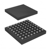
Packages Available– 32-lead PLCC– 32-lead TSOP (8mm x 14mm)
All non-Pb (lead-free) devices are RoHS compliant
The SST49LF080A flash memory device is designed to interface with the LPC bus for PC and Internet Appliance application in compliance with Intel Low Pin Count (LPC) Interface Specification 1.0. Two interface modes are supported: LPC mode for in-system operations and Parallel Programming (PP) mode to interface with programming equipment. The SST49LF080A flash memory device is manufactured with SST's proprietary, high-performance SuperFlash Technology. The split-gate cell design and thick-oxide tunneling injector attain better reliability and manufacturability compared with alternate approaches.
Additional Features
- LPC Interface Flash– SST49LF080A: 1024K x8 (8 Mbit)
- Conforms to Intel LPC Interface Specification 1.0
- Flexible Erase Capability– Uniform 4 KByte Sectors– Uniform 64 KByte overlay blocks– 64 KByte Top Boot Block protection– Chip-Erase for PP Mode Only
- Single 3.0-3.6V Read and Write Operations
- Superior Reliability– Endurance: 100,000 Cycles (typical)– Greater than 100 years Data Retention
- Low Power Consumption– Active Read Current: 6 mA (typical)– Standby Current: 10 µA (typical)
- Fast Sector-Erase/Byte-Program Operation– Sector-Erase Time: 18 ms (typical)– Block-Erase Time: 18 ms (typical)– Chip-Erase Time: 70 ms (typical)– Byte-Program Time: 14 µs (typical)– Chip Rewrite Time: 16 seconds (typical)– Single-pulse Program or Erase– Internal timing generation
- Two Operational Modes– Low Pin Count (LPC) Interface mode forin-system operation– Parallel Programming (PP) Mode for fast productionprogramming
- LPC Interface Mode– 5-signal communication interface supportingbyte Read and Write– 33 MHz clock frequency operation– WP# and TBL# pins provide hardware write protectfor entire chip and/or top boot block– Standard SDP Command Set– Data# Polling and Toggle Bit for End-of-Writedetection– 5 GPI pins for system design flexibility– 4 ID pins for multi-chip selection
- Parallel Programming (PP) Mode– 11-pin multiplexed address and 8-pin dataI/O interface– Supports fast programming In-System onprogrammer equipment
- CMOS and PCI I/O Compatibility
- Packages Available– 32-lead PLCC– 32-lead TSOP (8mm x 14mm)
- All non-Pb (lead-free) devices are RoHS compliant