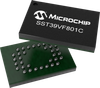
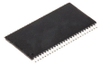
The SST39VF801C device is 512K x16 CMOS Multi-Purpose Flash Plus (MPF+) manufactured with SST proprietary, high performance CMOS SuperFlash technology. The split-gate cell design and thick-oxide tunneling injector attain better reliability and manufacturability compared with alternate approaches. The SST39VF801C writes (Program or Erase) with a 2.7-3.6V power supply. This device conforms to JEDEC standard pinouts for x16 memories.
Additional Features
Organized as 512K x16
Low Power Consumption (typical values at 5 MHz)– Active Current: 5 mA (typical)– Standby Current: 3 µA (typical)– Auto Low Power Mode: 3 µA (typical)
Hardware Block-Protection/WP# Input Pin– Top Block-Protection (top 8 KWord)– Bottom Block-Protection (bottom 8 KWord)
Sector-Erase Capability– Uniform 2 KWord sectors
Block-Erase Capability– Flexible block architecture; one 8-, two 4-, one16-, and fifteen 32-KWord blocks
Chip-Erase Capability
Erase-Suspend/Erase-
Resume Capabilities
Hardware Reset Pin (RST#)
Latched Address and Data
Security-ID Feature– SST: 128 bits; User: 128 words
Fast Erase and Word-Program:– Sector-Erase Time: 18 ms (typical)– Block-Erase Time: 18 ms (typical)– Chip-Erase Time: 40 ms (typical)– Word-Program Time: 7 µs (typical)
Automatic Write Timing– Internal VPP Generation
End-of-Write Detection– Toggle Bits– Data# Polling– Ready/Busy# Pin
CMOS I/O Compatibility
JEDEC Standard– Flash EEPROM Pinouts and command sets
Packages Available– 48-lead TSOP (12mm x 20mm)– 48-ball TFBGA (6mm x 8mm)– 48-ball WFBGA (4mm x 6mm)
The SST39VF801C device is 512K x16 CMOS Multi-Purpose Flash Plus (MPF+) manufactured with SST proprietary, high performance CMOS SuperFlash technology. The split-gate cell design and thick-oxide tunneling injector attain better reliability and manufacturability compared with alternate approaches. The SST39VF801C writes (Program or Erase) with a 2.7-3.6V power supply. This device conforms to JEDEC standard pinouts for x16 memories.
Additional Features
- Organized as 512K x16
- Low Power Consumption (typical values at 5 MHz)– Active Current: 5 mA (typical)– Standby Current: 3 µA (typical)– Auto Low Power Mode: 3 µA (typical)
- Hardware Block-Protection/WP# Input Pin– Top Block-Protection (top 8 KWord)– Bottom Block-Protection (bottom 8 KWord)
- Sector-Erase Capability– Uniform 2 KWord sectors
- Block-Erase Capability– Flexible block architecture; one 8-, two 4-, one16-, and fifteen 32-KWord blocks
- Chip-Erase Capability
- Erase-Suspend/Erase-Resume Capabilities
- Hardware Reset Pin (RST#)
- Latched Address and Data
- Security-ID Feature– SST: 128 bits; User: 128 words
- Fast Erase and Word-Program:– Sector-Erase Time: 18 ms (typical)– Block-Erase Time: 18 ms (typical)– Chip-Erase Time: 40 ms (typical)– Word-Program Time: 7 µs (typical)
- Automatic Write Timing– Internal VPP Generation
- End-of-Write Detection– Toggle Bits– Data# Polling– Ready/Busy# Pin
- CMOS I/O Compatibility
- JEDEC Standard– Flash EEPROM Pinouts and command sets
- Packages Available– 48-lead TSOP (12mm x 20mm)– 48-ball TFBGA (6mm x 8mm)– 48-ball WFBGA (4mm x 6mm)