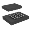
Microchip Technology, Inc. 2Mb 2.7-3.6V Parallel Flash SST39VF020

Description
The SST39VF020 is a 256K x8CMOS Multi-Purpose Flash (MPF) manufactured with SST proprietary, high performance CMOS SuperFlash technology. The split-gate cell design and thick-oxide tunneling injector attain better reliability and manufacturability compared with alternate approaches. The SST39VF020 device writes (Program or Erase) with a 2.7-3.6V power supply. The device conforms to JEDEC standard pinouts for x8 memories. Additional Features Organized as 64K x8 / 128K x8 / 256K x8 / 512K x8 Single Voltage Read and Write Operations– 3.0-3.6V for SST39LF512/010/020/0 40– 2.7-3.6V for SST39VF512/010/020/0 40 Superior Reliability– Endurance: 100,000 Cycles (typical)– Greater than 100 years Data Retention Low Power Consumption(typical values at 14 MHz)– Active Current: 5 mA (typical)– Standby Current: 1 µA (typical) Sector-Erase Capability– Uniform 4 KByte sectors Fast Read Access Time: 45 ns ; 55 ns ; 70 ns Latched Address and Data Fast Erase and Byte-Program:– Sector-Erase Time: 18 ms (typical)– Chip-Erase Time: 70 ms (typical)– Byte-Program Time: 14 µs (typical)– Chip Rewrite Time:4 seconds (typical) for SST39LF/VF020 Automatic Write Timing– Internal VPP Generation End-of-Write Detection– Toggle Bit– Data# Polling CMOS I/O Compatibility JEDEC Standard– Flash EEPROM Pinouts and command sets Packages Available– 32-lead PLCC– 32-lead TSOP (8mm x 14mm)– 48-ball TFBGA (6mm x 8mm)– 34-ball WFBGA (4mm x 6mm) for 1M and 2M All devices are RoHS compliant
Datasheet
Description
The SST39VF020 is a 256K x8CMOS Multi-Purpose Flash (MPF) manufactured with SST proprietary, high performance CMOS SuperFlash technology. The split-gate cell design and thick-oxide tunneling injector attain better reliability and manufacturability compared with alternate approaches. The SST39VF020 device writes (Program or Erase) with a 2.7-3.6V power supply. The device conforms to JEDEC standard pinouts for x8 memories. Additional Features Organized as 64K x8 / 128K x8 / 256K x8 / 512K x8 Single Voltage Read and Write Operations– 3.0-3.6V for SST39LF512/010/020/0 40– 2.7-3.6V for SST39VF512/010/020/0 40 Superior Reliability– Endurance: 100,000 Cycles (typical)– Greater than 100 years Data Retention Low Power Consumption(typical values at 14 MHz)– Active Current: 5 mA (typical)– Standby Current: 1 µA (typical) Sector-Erase Capability– Uniform 4 KByte sectors Fast Read Access Time: 45 ns ; 55 ns ; 70 ns Latched Address and Data Fast Erase and Byte-Program:– Sector-Erase Time: 18 ms (typical)– Chip-Erase Time: 70 ms (typical)– Byte-Program Time: 14 µs (typical)– Chip Rewrite Time:4 seconds (typical) for SST39LF/VF020 Automatic Write Timing– Internal VPP Generation End-of-Write Detection– Toggle Bit– Data# Polling CMOS I/O Compatibility JEDEC Standard– Flash EEPROM Pinouts and command sets Packages Available– 32-lead PLCC– 32-lead TSOP (8mm x 14mm)– 48-ball TFBGA (6mm x 8mm)– 34-ball WFBGA (4mm x 6mm) for 1M and 2M All devices are RoHS compliant
Datasheet

Suppliers

Company
Product
Description
Supplier Links
2Mb 2.7-3.6V Parallel Flash - SST39VF020 - Microchip Technology, Inc.
Chandler, AZ, United States
2Mb 2.7-3.6V Parallel Flash
SST39VF020
2Mb 2.7-3.6V Parallel Flash SST39VF020
The SST39VF020 is a 256K x8CMOS Multi-Purpose Flash (MPF) manufactured with SST proprietary, high performance CMOS SuperFlash technology. The split-gate cell design and thick-oxide tunneling injector attain better reliability and manufacturability compared with alternate approaches. The SST39VF020 device writes (Program or Erase) with a 2.7-3.6V power supply. The device conforms to JEDEC standard pinouts for x8 memories. Additional Features Organized as 64K x8 / 128K x8 / 256K x8 / 512K x8 Single Voltage Read and Write Operations– 3.0-3.6V for SST39LF512/010/020/0 40– 2.7-3.6V for SST39VF512/010/020/0 40 Superior Reliability– Endurance: 100,000 Cycles (typical)– Greater than 100 years Data Retention Low Power Consumption(typical values at 14 MHz)– Active Current: 5 mA (typical)– Standby Current: 1 µA (typical) Sector-Erase Capability– Uniform 4 KByte sectors Fast Read Access Time: 45 ns ; 55 ns ; 70 ns Latched Address and Data Fast Erase and Byte-Program:– Sector-Erase Time: 18 ms (typical)– Chip-Erase Time: 70 ms (typical)– Byte-Program Time: 14 µs (typical)– Chip Rewrite Time:4 seconds (typical) for SST39LF/VF020 Automatic Write Timing– Internal VPP Generation End-of-Write Detection– Toggle Bit– Data# Polling CMOS I/O Compatibility JEDEC Standard– Flash EEPROM Pinouts and command sets Packages Available– 32-lead PLCC– 32-lead TSOP (8mm x 14mm)– 48-ball TFBGA (6mm x 8mm)– 34-ball WFBGA (4mm x 6mm) for 1M and 2M All devices are RoHS compliant

The SST39VF020 is a 256K x8CMOS Multi-Purpose Flash (MPF) manufactured with SST proprietary, high performance CMOS SuperFlash technology. The split-gate cell design and thick-oxide tunneling injector attain better reliability and manufacturability compared with alternate approaches. The SST39VF020 device writes (Program or Erase) with a 2.7-3.6V power supply. The device conforms to JEDEC standard pinouts for x8 memories.

Additional Features

  • Organized as 64K x8 / 128K x8 / 256K x8 / 512K x8
  • Single Voltage Read and Write Operations– 3.0-3.6V for SST39LF512/010/020/040– 2.7-3.6V for SST39VF512/010/020/040
  • Superior Reliability– Endurance: 100,000 Cycles (typical)– Greater than 100 years Data Retention
  • Low Power Consumption(typical values at 14 MHz)– Active Current: 5 mA (typical)– Standby Current: 1 µA (typical)
  • Sector-Erase Capability– Uniform 4 KByte sectors
  • Fast Read Access Time: 45 ns ; 55 ns ; 70 ns
  • Latched Address and Data
  • Fast Erase and Byte-Program:– Sector-Erase Time: 18 ms (typical)– Chip-Erase Time: 70 ms (typical)– Byte-Program Time: 14 µs (typical)– Chip Rewrite Time:4 seconds (typical) for SST39LF/VF020
  • Automatic Write Timing– Internal VPP Generation
  • End-of-Write Detection– Toggle Bit– Data# Polling
  • CMOS I/O Compatibility
  • JEDEC Standard– Flash EEPROM Pinouts and command sets
  • Packages Available– 32-lead PLCC– 32-lead TSOP (8mm x 14mm)– 48-ball TFBGA (6mm x 8mm)– 34-ball WFBGA (4mm x 6mm) for 1M and 2M
  • All devices are RoHS compliant
Supplier's Site Datasheet

Technical Specifications

  Microchip Technology, Inc.
Product Category Memory Chips
Product Number SST39VF020
Product Name 2Mb 2.7-3.6V Parallel Flash
Memory Category Flash
Data Rate 0 MHz
Access Time 70 ns
Endurance 100000 Write/Erase Cycles
Unlock Full Specs
to access all available technical data

Similar Products

Memory - IS29GL512S-11TFV010 - Lingto Electronic Limited
Infineon Technologies AG
Specs
Memory Category Flash; Flash
Access Time 110 ns
Density 512000 kbits
View Details
2 suppliers
Flash Memory - 1882519 - RS Components, Ltd.
RS Components, Ltd.
Specs
Memory Category Flash
Bits per Word 8 bits
Pins 8
View Details
Memory - 71256L55TDB - Lingto Electronic Limited
Rochester Electronics
Specs
Memory Category SRAM; SRAM Chip
Access Time 55 ns
Density 256 kbits
View Details
Integrated Circuits (ICs) - Memory - Memory - 93Z667DMQB65 - Acme Chip Technology Co., Limited
Specs
Memory Category PROM; Non-Volatile
Cycle Time 65 ns
Density 64 kbits
View Details
2 suppliers