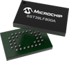
The SST39LF800A is a 512K x16 CMOS Multi-Purpose Flash (MPF) manufactured with SST proprietary, high performance CMOS SuperFlash technology. The split-gate cell design and thick oxide tunneling injector attain better reliability and manufacturability compared with alternate approaches. The SST39LF800A writes (Program or Erase) with a 3.0-3.6V power supply. This device conforms to JEDEC standard pinouts for x16 memories.
Please consider this device SST39LF801C, SST39LF802C
Additional Features
Organized as 512K x16
Single Voltage Read and Write Operations– 3.0-3.6V for SST39LF800A
Superior Reliability– Endurance: 100,000 Cycles (typical)– Greater than 100 years Data Retention
Low Power Consumption(typical values at 14 MHz)– Active Current: 9 mA (typical)– Standby Current: 3 µA (typical)
Sector-Erase Capability– Uniform 2 KWord sectors
Block-Erase Capability– Uniform 32 KWord blocks
Fast Read Access Time– 55 ns for SST39LF800A
Latched Address and Data
Fast Erase and Word-Program– Sector-Erase Time: 18 ms (typical)– Block-Erase Time: 18 ms (typical)– Chip-Erase Time: 70 ms (typical)– Word-Program Time: 14 µs (typical)– Chip Rewrite Time:8 seconds (typical) for SST39LF800A
Automatic Write Timing– Internal VPP Generation
End-of-Write Detection– Toggle Bit– Data# Polling
CMOS I/O Compatibility
JEDEC Standard– Flash EEPROM Pinouts and command sets
Packages Available– 48-lead TSOP (12mm x 20mm)– 48-ball TFBGA (6mm x 8mm)– 48-ball WFBGA (4mm x 6mm)– 48-bump XFLGA (4mm x 6mm) – 4 and 8Mbit
All non-Pb (lead-free) devices are RoHS compliant
The SST39LF800A is a 512K x16 CMOS Multi-Purpose Flash (MPF) manufactured with SST proprietary, high performance CMOS SuperFlash technology. The split-gate cell design and thick oxide tunneling injector attain better reliability and manufacturability compared with alternate approaches. The SST39LF800A writes (Program or Erase) with a 3.0-3.6V power supply. This device conforms to JEDEC standard pinouts for x16 memories.
Please consider this device SST39LF801C, SST39LF802C
Additional Features
- Organized as 512K x16
- Single Voltage Read and Write Operations– 3.0-3.6V for SST39LF800A
- Superior Reliability– Endurance: 100,000 Cycles (typical)– Greater than 100 years Data Retention
- Low Power Consumption(typical values at 14 MHz)– Active Current: 9 mA (typical)– Standby Current: 3 µA (typical)
- Sector-Erase Capability– Uniform 2 KWord sectors
- Block-Erase Capability– Uniform 32 KWord blocks
- Fast Read Access Time– 55 ns for SST39LF800A
- Latched Address and Data
- Fast Erase and Word-Program– Sector-Erase Time: 18 ms (typical)– Block-Erase Time: 18 ms (typical)– Chip-Erase Time: 70 ms (typical)– Word-Program Time: 14 µs (typical)– Chip Rewrite Time:8 seconds (typical) for SST39LF800A
- Automatic Write Timing– Internal VPP Generation
- End-of-Write Detection– Toggle Bit– Data# Polling
- CMOS I/O Compatibility
- JEDEC Standard– Flash EEPROM Pinouts and command sets
- Packages Available– 48-lead TSOP (12mm x 20mm)– 48-ball TFBGA (6mm x 8mm)– 48-ball WFBGA (4mm x 6mm)– 48-bump XFLGA (4mm x 6mm) – 4 and 8Mbit
- All non-Pb (lead-free) devices are RoHS compliant