Microchip Technology, Inc. Differential Programmable Clock PL611-31

Description
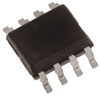
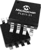
CREATE AND SAMPLE YOUR CUSTOM PL611 HERE The PL611-31-xxx is a low-cost, general purpose frequency synthesizer and a member of Micrel’s factoryprogrammable Quick Turn Clock (QTC) family. The PL611-31-xxx product family can generate any output frequency up to 200MHz from a fundamental crystal input of 10MHz to 30MHz. In addition, the complementary LVCMOS outputs can be used to drive differential LVPECL, LVDS, HCSL or CML inputs at 2.5V or 3.3V. Additional Features Advanced programmable PLL design Very low jitter and phase noise (<40ps peak-to-peak typical) Up to 3 outputs Output frequency up to 200MHz CMOS Provides complementary LVCMOS outputs to drive LVCMOS, LVPECL, LVDS, HCSL or CML inputs Input frequencies: Fundamental crystal: 10MHz – 30MHz Reference clock: 1MHz – 200MHz Accepts <1.0V reference signal input voltage One programmable I/O pin can be configured as output enable (OE) input, frequency selection (FSEL) input, or reference clock output Single 2.5V ~ 3.3V ±10% power supply Operating temperature range from –40°C to +85°C Available in 8-pin SOICN, GREEN/RoHS-compliant package
Datasheet
Description
CREATE AND SAMPLE YOUR CUSTOM PL611 HERE The PL611-31-xxx is a low-cost, general purpose frequency synthesizer and a member of Micrel’s factoryprogrammable Quick Turn Clock (QTC) family. The PL611-31-xxx product family can generate any output frequency up to 200MHz from a fundamental crystal input of 10MHz to 30MHz. In addition, the complementary LVCMOS outputs can be used to drive differential LVPECL, LVDS, HCSL or CML inputs at 2.5V or 3.3V. Additional Features Advanced programmable PLL design Very low jitter and phase noise (<40ps peak-to-peak typical) Up to 3 outputs Output frequency up to 200MHz CMOS Provides complementary LVCMOS outputs to drive LVCMOS, LVPECL, LVDS, HCSL or CML inputs Input frequencies: Fundamental crystal: 10MHz – 30MHz Reference clock: 1MHz – 200MHz Accepts <1.0V reference signal input voltage One programmable I/O pin can be configured as output enable (OE) input, frequency selection (FSEL) input, or reference clock output Single 2.5V ~ 3.3V ±10% power supply Operating temperature range from –40°C to +85°C Available in 8-pin SOICN, GREEN/RoHS-compliant package
Datasheet

Suppliers

Company
Product
Description
Supplier Links
Differential Programmable Clock - PL611-31 - Microchip Technology, Inc.
Chandler, AZ, United States
Differential Programmable Clock
PL611-31
Differential Programmable Clock PL611-31
CREATE AND SAMPLE YOUR CUSTOM PL611 HERE The PL611-31-xxx is a low-cost, general purpose frequency synthesizer and a member of Micrel’s factoryprogrammable Quick Turn Clock (QTC) family. The PL611-31-xxx product family can generate any output frequency up to 200MHz from a fundamental crystal input of 10MHz to 30MHz. In addition, the complementary LVCMOS outputs can be used to drive differential LVPECL, LVDS, HCSL or CML inputs at 2.5V or 3.3V. Additional Features Advanced programmable PLL design Very low jitter and phase noise (<40ps peak-to-peak typical) Up to 3 outputs Output frequency up to 200MHz CMOS Provides complementary LVCMOS outputs to drive LVCMOS, LVPECL, LVDS, HCSL or CML inputs Input frequencies: Fundamental crystal: 10MHz – 30MHz Reference clock: 1MHz – 200MHz Accepts <1.0V reference signal input voltage One programmable I/O pin can be configured as output enable (OE) input, frequency selection (FSEL) input, or reference clock output Single 2.5V ~ 3.3V ±10% power supply Operating temperature range from –40°C to +85°C Available in 8-pin SOICN, GREEN/RoHS-compliant package

CREATE AND SAMPLE YOUR CUSTOM PL611 HERE

The PL611-31-xxx is a low-cost, general purpose frequency synthesizer and a member of Micrel’s factoryprogrammable Quick Turn Clock (QTC) family. The PL611-31-xxx product family can generate any output frequency up to 200MHz from a fundamental crystal input of 10MHz to 30MHz. In addition, the complementary LVCMOS outputs can be used to drive differential LVPECL, LVDS, HCSL or CML inputs at 2.5V or 3.3V.

Additional Features

    • Advanced programmable PLL design
    • Very low jitter and phase noise (<40ps peak-to-peak typical)
    • Up to 3 outputs
    • Output frequency up to 200MHz CMOS
      • Provides complementary LVCMOS outputs to drive LVCMOS, LVPECL, LVDS, HCSL or CML inputs
    • Input frequencies:
      • Fundamental crystal: 10MHz – 30MHz
      • Reference clock: 1MHz – 200MHz
    • Accepts <1.0V reference signal input voltage
    • One programmable I/O pin can be configured as output enable (OE) input, frequency selection (FSEL) input, or reference clock output
    • Single 2.5V ~ 3.3V ±10% power supply
    • Operating temperature range from –40°C to +85°C
    • Available in 8-pin SOICN, GREEN/RoHS-compliant package
Supplier's Site Datasheet

Technical Specifications

  Microchip Technology, Inc.
Product Category IC Clocks
Product Number PL611-31
Product Name Differential Programmable Clock
Device Type Clock Generator
Unlock Full Specs
to access all available technical data

Similar Products

 - SIT8924BE-73-33N-48.000000G - Rochester Electronics
Specs
Device Type Real Time Clock
Bus Interface CMOS
Features / Standards RoHS
View Details
CDCVF2505 PLL Clock Driver for Synch. DRAM & Gen. Purp. Apps W/Spread Spectrum Compatibility, Power Down Mode - CDCVF2505D - Texas Instruments
Specs
Device Type Clock Driver
Package Type SOIC,TSSOP
Supply Voltage 3.3 volts
View Details
8 suppliers
Clock and Timing IC - 763-SI5017-D-GMR - ERSAELECTRONICS PTE. LTD.
Skyworks Solutions, Inc.
Specs
Bus Interface CML
Package Type Tape & Reel (TR)
Supply Voltage 3.13 to 3.46 volts
View Details
2 suppliers