The PIC24H 16-bit device family employs a powerful 16-bit architecture, ideal for applications that rely on high-speed, repetitive computations, as well as control. The devices are pin compatible with the dsPIC33F family of devices, and share a very high degree of compatibility with the dsPIC30F family devices. This allows seamless migration options from/to PIC24F, dsPIC30F and dsPIC33F devices.
Additional Features
Operating Range
Up to 40 MIPS operation (3.0-3.6V)
Industrial temperature range (-40°C to +85°C)
Extended temperature range (-40°C to +125°C)
High Efficiency PIC24H core
Modified Harvard architecture
C compiler optimized instruction set
16-bit-wide data path, 24-bit-wide instructions
Linear program memory addressing up to 4M instruction words
Linear data memory addressing up to 64 Kbytes
71 base instructions, mostly one word/one cycle
Sixteen 16-bit general purpose registers
Flexible and powerful addressing modes
16 x 16 multiply operations
32/16 and 16/16 divide operations
Up to ±16-bit shifts for up to 40-bit data
Interrupt Controller
5-cycle latency
Up to 21 available interrupt sources
Up to three external interrupts
Seven programmable priority levels
Four processor exceptions
Digital I/O
Peripheral Pin Select Functionality
Up to 21 programmable digital I/O pins
Wake-up/Interrupt-on
-Change for up to 21 pins
Output pins can drive from 3.0V to 3.6V
Up to 5V output with open drain configurations on 5V tolerant pins
4 mA sink on all I/O pins
System Management
Flexible clock options: - External, crystal, resonator, internal RC, fully integrated Phase-Locked Loop (PLL) and extremely low-jitter PLL
Power-up Timer
Oscillator Start-up Timer/Stabilizer
Watchdog Timer with its own RC oscillator
Fail-Safe Clock Monitor (FSCM)
Reset by multiple sources
Power Management
On-chip 2.5V voltage regulator
Switch between clock sources in real time
Idle, Sleep, and Doze modes with fast wake-up
Timers/Capture/Compa
re
Timer/Counters, up to three 16-bit timers: - Can pair up to make one 32-bit timer, one timer runs as Real-Time Clock with external 32.768 kHz oscillator and programmable prescaler
Input Capture (up to four channels): - Capture on up, down, or both edges, 16-bit capture input functions and 4-deep FIFO on each capture
Output Compare (up to two channels): - Single or Dual 16-bit Compare mode, 16-bit Glitchless PWM Mode
Communication Modules
4-wire SPI with framing supports I/O interface to simple codecs, supports 8-bit and 16-bit data and all serial clock formats and sampling modes
I2C™ with Full Multi-Master Slave mode support, 7-bit and 10-bit addressing, bus collision detection and arbitration, integrated signal conditioning, slave address masking
UART with LIN bus support, IrDA® encoding and decoding in hardware, High-Speed Baud Mode, Hardware Flow Control with CTS and RTS
Analog-to-Digital Converters (ADCs)
10-bit, 1.1 Msps or 12-bit, 500 Ksps conversion
Two and four simultaneous samples (10-bit ADC)
Up to 10 input channels with auto-scanning
Conversion start can be manual or synchronized with one of four trigger sources
Conversion possible in Sleep mode
±2 LSb max integral nonlinearity
±1 LSb max differential nonlinearity
Packaging
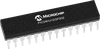
18-pin PDIP/SOIC
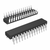
28-pin SPDIP/SOIC/QFN/SSOP
The PIC24H 16-bit device family employs a powerful 16-bit architecture, ideal for applications that rely on high-speed, repetitive computations, as well as control. The devices are pin compatible with the dsPIC33F family of devices, and share a very high degree of compatibility with the dsPIC30F family devices. This allows seamless migration options from/to PIC24F, dsPIC30F and dsPIC33F devices.
Additional Features
- Operating Range
- Up to 40 MIPS operation (3.0-3.6V)
- Industrial temperature range (-40°C to +85°C)
- Extended temperature range (-40°C to +125°C)
- High Efficiency PIC24H core
- Modified Harvard architecture
- C compiler optimized instruction set
- 16-bit-wide data path, 24-bit-wide instructions
- Linear program memory addressing up to 4M instruction words
- Linear data memory addressing up to 64 Kbytes
- 71 base instructions, mostly one word/one cycle
- Sixteen 16-bit general purpose registers
- Flexible and powerful addressing modes
- 16 x 16 multiply operations
- 32/16 and 16/16 divide operations
- Up to ±16-bit shifts for up to 40-bit data
- Interrupt Controller
- 5-cycle latency
- Up to 21 available interrupt sources
- Up to three external interrupts
- Seven programmable priority levels
- Four processor exceptions
- Digital I/O
- Peripheral Pin Select Functionality
- Up to 21 programmable digital I/O pins
- Wake-up/Interrupt-on-Change for up to 21 pins
- Output pins can drive from 3.0V to 3.6V
- Up to 5V output with open drain configurations on 5V tolerant pins
- 4 mA sink on all I/O pins
- System Management
- Flexible clock options: - External, crystal, resonator, internal RC, fully integrated Phase-Locked Loop (PLL) and extremely low-jitter PLL
- Power-up Timer
- Oscillator Start-up Timer/Stabilizer
- Watchdog Timer with its own RC oscillator
- Fail-Safe Clock Monitor (FSCM)
- Reset by multiple sources
- Power Management
- On-chip 2.5V voltage regulator
- Switch between clock sources in real time
- Idle, Sleep, and Doze modes with fast wake-up
- Timers/Capture/Compare
- Timer/Counters, up to three 16-bit timers: - Can pair up to make one 32-bit timer, one timer runs as Real-Time Clock with external 32.768 kHz oscillator and programmable prescaler
- Input Capture (up to four channels): - Capture on up, down, or both edges, 16-bit capture input functions and 4-deep FIFO on each capture
- Output Compare (up to two channels): - Single or Dual 16-bit Compare mode, 16-bit Glitchless PWM Mode
- Communication Modules
- 4-wire SPI with framing supports I/O interface to simple codecs, supports 8-bit and 16-bit data and all serial clock formats and sampling modes
- I2C™ with Full Multi-Master Slave mode support, 7-bit and 10-bit addressing, bus collision detection and arbitration, integrated signal conditioning, slave address masking
- UART with LIN bus support, IrDA® encoding and decoding in hardware, High-Speed Baud Mode, Hardware Flow Control with CTS and RTS
- Analog-to-Digital Converters (ADCs)
- 10-bit, 1.1 Msps or 12-bit, 500 Ksps conversion
- Two and four simultaneous samples (10-bit ADC)
- Up to 10 input channels with auto-scanning
- Conversion start can be manual or synchronized with one of four trigger sources
- Conversion possible in Sleep mode
- ±2 LSb max integral nonlinearity
- ±1 LSb max differential nonlinearity
- Packaging
- 18-pin PDIP/SOIC
- 28-pin SPDIP/SOIC/QFN/SSOP