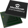
The Microchip's ARM®-based SAM9N12 is an ARM926EJ-S based microprocessor running at 400MHz. Its extensive peripheral set includes an integrated graphics LCD controller that supports screen resolutions up to WVGA with 16M colors and 24bpp. In addition, it offers support for a wide range of external memories, including LPDDR/DDR2 and MLC NAND flash memory with up to 24-bit ECC. The SAM9N12 features multiple communication interfaces, such as a Full Speed USB host and device with on-chip transceivers, SD/SDIO/MMC, USARTs, SPIs, I2S and I2C. The device is available in a 217-ball BGA package with 0.8mm ball pitch as well as a 247-ball BGA package with 0.5mm ball pitch.
Additional Features
Core:
ARM926EJ-S ARM® Thumb® Processor running up to 400 MHz
16 Kbytes Data Cache, 16 Kbytes Instruction Cache, Memory Management Unit Memories
One 128-Kbyte internal ROM embedding standard or secure bootstrap routine
One 32-Kbyte internal SRAM, single-cycle access at system speed
32-bit External Bus Interface supporting 8-bank DDR2/LPDDR, SDR/LPSDR, Static Memories
MLC/SLC NAND Controller, with up to 24-bit Programmable Multibit Error Correction Code (PMECC) System running up to 133 MHz
Power-on Reset, Reset Controller, Shutdown Controller, Periodic Interval Timer, Watchdog Timer and Real Time Clock
Boot Mode Select Option, Remap Command
Internal Low Power 32 kHz RC and Fast 12 MHz RC Oscillators
Selectable 32768 Hz Low-power Oscillator, 16 MHz Oscillator, one PLL for the system and one PLL optimized for USB
Six 32-bit-layer AHB Bus Matrix
Dual Peripheral Bridge with dedicated programmable clock
One dual port 8-channel DMA Controller
Advanced Interrupt Controller (AIC)
Two Programmable External Clock Signals
Low-power Mode
Shutdown Controller with four 32-bit General-purpose Backup Registers
Clock Generator and Power Management Controller
Very Slow Clock Operating Mode, Software Programmable Power Optimization Capabilities
Peripherals:
LCD Controller
USB Device Full Speed with dedicated On-chip Transceiver
USB Host Full Speed with dedicated On-chip Transceiver
One High-speed SD card and SDIO Host Controller
Two Master/Slave Serial Peripheral Interfaces (SPI)
Two 3-channel 32-bit Timer/Counters (TC)
One Synchronous Serial Controller (SSC)
One 4-channel 16-bit PWM Controller
Two 2-wire Interfaces (TWI)
Four Universal Synchronous Asynchronous Receiver Transmitters (USART)
Two Universal Asynchronous Receiver Transmitters (UART)
One Debug Unit (DBGU)
One 12-channel 10-bit Analog-to-Digital Converter with up to 5-wire resistive Touchscreen support
Safety:
Crystal Failure Detection
Independent Watchdog
Power-on Reset Cells
Register Write Protection
SHA (SHA1 and SHA256) Compliant with FIPS Publication 180-2 (SAM9CN11/SAM9CN12 devices)
Cryptography:
True Random Number Generator (TRNG) compliant with NIST Special Publication 800-22
AES 256-, 192-, 128-bit Key Algorithm compliant with FIPS Publication 197 (SAM9CN11/SAM9CN12 devices)
256 Fuse bits for crypto key and 64 Fuse bits for device configuration, including JTAG disable and forced boot from the on-chip ROM (Secure Boot feature - SAM9CN12 only)
I/O:
Four 32-bit Parallel Input/Output Controllers
105 Programmable I/O Lines Multiplexed with up to Three Peripheral I/Os
Input Change Interrupt Capability on Each I/O Line, optional Schmitt Trigger input
Individually Programmable Open-drain, Pull-up and Pull-down Resistor, Synchronous Output
Packages:
217-ball BGA, pitch 0.8 mm
247-ball BGA, pitch 0.5 mm
The Microchip's ARM®-based SAM9N12 is an ARM926EJ-S based microprocessor running at 400MHz. Its extensive peripheral set includes an integrated graphics LCD controller that supports screen resolutions up to WVGA with 16M colors and 24bpp. In addition, it offers support for a wide range of external memories, including LPDDR/DDR2 and MLC NAND flash memory with up to 24-bit ECC. The SAM9N12 features multiple communication interfaces, such as a Full Speed USB host and device with on-chip transceivers, SD/SDIO/MMC, USARTs, SPIs, I2S and I2C. The device is available in a 217-ball BGA package with 0.8mm ball pitch as well as a 247-ball BGA package with 0.5mm ball pitch.
Additional Features
- Core:
- ARM926EJ-S ARM® Thumb® Processor running up to 400 MHz
- 16 Kbytes Data Cache, 16 Kbytes Instruction Cache, Memory Management Unit Memories
- One 128-Kbyte internal ROM embedding standard or secure bootstrap routine
- One 32-Kbyte internal SRAM, single-cycle access at system speed
- 32-bit External Bus Interface supporting 8-bank DDR2/LPDDR, SDR/LPSDR, Static Memories
- MLC/SLC NAND Controller, with up to 24-bit Programmable Multibit Error Correction Code (PMECC) System running up to 133 MHz
- Power-on Reset, Reset Controller, Shutdown Controller, Periodic Interval Timer, Watchdog Timer and Real Time Clock
- Boot Mode Select Option, Remap Command
- Internal Low Power 32 kHz RC and Fast 12 MHz RC Oscillators
- Selectable 32768 Hz Low-power Oscillator, 16 MHz Oscillator, one PLL for the system and one PLL optimized for USB
- Six 32-bit-layer AHB Bus Matrix
- Dual Peripheral Bridge with dedicated programmable clock
- One dual port 8-channel DMA Controller
- Advanced Interrupt Controller (AIC)
- Two Programmable External Clock Signals
- Low-power Mode
- Shutdown Controller with four 32-bit General-purpose Backup Registers
- Clock Generator and Power Management Controller
- Very Slow Clock Operating Mode, Software Programmable Power Optimization Capabilities
- Peripherals:
- LCD Controller
- USB Device Full Speed with dedicated On-chip Transceiver
- USB Host Full Speed with dedicated On-chip Transceiver
- One High-speed SD card and SDIO Host Controller
- Two Master/Slave Serial Peripheral Interfaces (SPI)
- Two 3-channel 32-bit Timer/Counters (TC)
- One Synchronous Serial Controller (SSC)
- One 4-channel 16-bit PWM Controller
- Two 2-wire Interfaces (TWI)
- Four Universal Synchronous Asynchronous Receiver Transmitters (USART)
- Two Universal Asynchronous Receiver Transmitters (UART)
- One Debug Unit (DBGU)
- One 12-channel 10-bit Analog-to-Digital Converter with up to 5-wire resistive Touchscreen support
- Safety:
- Crystal Failure Detection
- Independent Watchdog
- Power-on Reset Cells
- Register Write Protection
- SHA (SHA1 and SHA256) Compliant with FIPS Publication 180-2 (SAM9CN11/SAM9CN12 devices)
- Cryptography:
- True Random Number Generator (TRNG) compliant with NIST Special Publication 800-22
- AES 256-, 192-, 128-bit Key Algorithm compliant with FIPS Publication 197 (SAM9CN11/SAM9CN12 devices)
- 256 Fuse bits for crypto key and 64 Fuse bits for device configuration, including JTAG disable and forced boot from the on-chip ROM (Secure Boot feature - SAM9CN12 only)
- I/O:
- Four 32-bit Parallel Input/Output Controllers
- 105 Programmable I/O Lines Multiplexed with up to Three Peripheral I/Os
- Input Change Interrupt Capability on Each I/O Line, optional Schmitt Trigger input
- Individually Programmable Open-drain, Pull-up and Pull-down Resistor, Synchronous Output
- Packages:
- 217-ball BGA, pitch 0.8 mm
- 247-ball BGA, pitch 0.5 mm