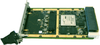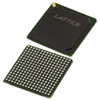
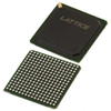
Lattice Semiconductor Corporation FPGAs (Field Programmable Gate Array) LFSCM3GA15EP1-5FN256I

Description
SCM Field Programmable Gate Array (FPGA) IC 139 1054720 15000 256-BGA
Description
SCM Field Programmable Gate Array (FPGA) IC 139 1054720 15000 256-BGA
Datasheet
Datasheet Summary
Powered by GS/AI

The LFSCM3GA15EP1-5FN256I is a member of the LatticeSC/M family of FPGAs, featuring a high-performance FPGA fabric with 15K Look-Up Tables (LUTs) and a maximum of 256 I/O pins. It supports a range of embedded memory options, including up to 7.8 Mbits of sysMEM block RAM and additional distributed RAM. The device operates at a core voltage of 1.2V and is packaged in a lead-free 256-ball fpBGA format. This FPGA includes advanced clock management capabilities with eight analog PLLs and twelve DLLs, enabling clock frequencies from 15MHz to 1GHz. It also features high-speed SERDES with performance ranging from 600Mbps to 3.8Gbps, suitable for various communication standards such as GbE and PCI Express. The device supports multiple I/O standards, including LVCMOS, LVTTL, and LVDS, with programmable on-die termination options. The LFSCM3GA15EP1-5FN256I is designed for applications requiring high performance and flexibility, making it suitable for complex system designs in communication and data processing.

Datasheet Summary
Powered by GS/AI

The LFSCM3GA15EP1-5FN256I is a member of the LatticeSC/M family of FPGAs, featuring a high-performance FPGA fabric with 15K Look-Up Tables (LUTs) and a maximum of 256 I/O pins. It supports a range of embedded memory options, including up to 7.8 Mbits of sysMEM block RAM and additional distributed RAM. The device operates at a core voltage of 1.2V and is packaged in a lead-free 256-ball fpBGA format. This FPGA includes advanced clock management capabilities with eight analog PLLs and twelve DLLs, enabling clock frequencies from 15MHz to 1GHz. It also features high-speed SERDES with performance ranging from 600Mbps to 3.8Gbps, suitable for various communication standards such as GbE and PCI Express. The device supports multiple I/O standards, including LVCMOS, LVTTL, and LVDS, with programmable on-die termination options. The LFSCM3GA15EP1-5FN256I is designed for applications requiring high performance and flexibility, making it suitable for complex system designs in communication and data processing.

Suppliers

Company
Product
Description
Supplier Links
FPGAs (Field Programmable Gate Array) - LFSCM3GA15EP1-5FN256I - Quarktwin Technology Ltd.
Shenzhen, Guangdong, China
FPGAs (Field Programmable Gate Array)
LFSCM3GA15EP1-5FN256I
FPGAs (Field Programmable Gate Array) LFSCM3GA15EP1-5FN256I
SCM Field Programmable Gate Array (FPGA) IC 139 1054720 15000 256-BGA

SCM Field Programmable Gate Array (FPGA) IC 139 1054720 15000 256-BGA

Buy Now Datasheet
Embedded - FPGAs (Field Programmable Gate Array) - LFSCM3GA15EP1-5FN256I - Lingto Electronic Limited
Shenzhen, China
Embedded - FPGAs (Field Programmable Gate Array)
LFSCM3GA15EP1-5FN256I
Embedded - FPGAs (Field Programmable Gate Array) LFSCM3GA15EP1-5FN256I
IC FPGA 139 I/O 256FBGA

IC FPGA 139 I/O 256FBGA

Supplier's Site Datasheet

Technical Specifications

  Quarktwin Technology Ltd. Lingto Electronic Limited
Product Category Field-Programmable Gate Arrays (FPGA) Field-Programmable Gate Arrays (FPGA)
Product Number LFSCM3GA15EP1-5FN256I LFSCM3GA15EP1-5FN256I
Product Name FPGAs (Field Programmable Gate Array) Embedded - FPGAs (Field Programmable Gate Array)
Logic Cells / Logic Blocks 15000 15000
Package Type Other; 256-BGA
User I/Os 139 pins 139 pins
Unlock Full Specs
to access all available technical data