Integrated Device Technology FemtoClock NG Jitter Attenuator and Clock Synthesizer 8V19N407Z-24NLGI8

Description
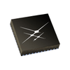
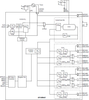
8V19N407Z -24 is a fully integrated FemtoClock® NG Jitter Attenuator and Clock Synthesizer. The device is a high-performance clock solution for conditioning and frequency/phase management of wireless base station radio equipment boards and is optimized to deliver excellent phase noise performance. The device supports JESD204B subclass 0 and 1 clock implementations. The device is very flexible in programming of the output frequency and phase. A two-stage PLL architecture supports both jitter attenuation and frequency multiplication. The first stage PLL is the jitter attenuator and uses an external VCXO for best possible phase noise characteristics.The second stage PLL lock on the VCXO - PLL output signal and synthesizes the target frequency. The second-stage PLL use an internal VCO . The device supports the clock generation of high-frequency clocks from the VCO and low-frequency system reference signals ( SYSREF ). The system reference signals are internally synchronized to the clock signals. Delay functions exist for achieving alignment and controlled phase delay between system reference and clock signals and to align/delay individual output signals. The input is monitored for activity. The “hold-over” is provided to handle clock input failure scenarios. Auto-lock, individually programmable output frequency dividers and phase adjustment capabilities are added for flexibility. The device is configured through a 4-wire SP serial interface and reports lock and signal loss status in internal registers and optionally via an lock detect (nINT) output. The device is packaged in a lead-free (RoHS 6) 72-lead VFQFN package. The extended temperature range supports wireless infrastructure, telecommunication and networking end equipment requirements. The device is a member of the high-performance clock family from IDT . For information regarding evaluation boards and material, please contact your local IDT sales representative.
Description
8V19N407Z -24 is a fully integrated FemtoClock® NG Jitter Attenuator and Clock Synthesizer. The device is a high-performance clock solution for conditioning and frequency/phase management of wireless base station radio equipment boards and is optimized to deliver excellent phase noise performance. The device supports JESD204B subclass 0 and 1 clock implementations. The device is very flexible in programming of the output frequency and phase. A two-stage PLL architecture supports both jitter attenuation and frequency multiplication. The first stage PLL is the jitter attenuator and uses an external VCXO for best possible phase noise characteristics.The second stage PLL lock on the VCXO - PLL output signal and synthesizes the target frequency. The second-stage PLL use an internal VCO . The device supports the clock generation of high-frequency clocks from the VCO and low-frequency system reference signals ( SYSREF ). The system reference signals are internally synchronized to the clock signals. Delay functions exist for achieving alignment and controlled phase delay between system reference and clock signals and to align/delay individual output signals. The input is monitored for activity. The “hold-over” is provided to handle clock input failure scenarios. Auto-lock, individually programmable output frequency dividers and phase adjustment capabilities are added for flexibility. The device is configured through a 4-wire SP serial interface and reports lock and signal loss status in internal registers and optionally via an lock detect (nINT) output. The device is packaged in a lead-free (RoHS 6) 72-lead VFQFN package. The extended temperature range supports wireless infrastructure, telecommunication and networking end equipment requirements. The device is a member of the high-performance clock family from IDT . For information regarding evaluation boards and material, please contact your local IDT sales representative.

Suppliers

Company
Product
Description
Supplier Links
FemtoClock NG Jitter Attenuator and Clock Synthesizer - 8V19N407Z-24NLGI8 - Integrated Device Technology
San Jose, CA, USA
FemtoClock NG Jitter Attenuator and Clock Synthesizer
8V19N407Z-24NLGI8
FemtoClock NG Jitter Attenuator and Clock Synthesizer 8V19N407Z-24NLGI8
8V19N407Z -24 is a fully integrated FemtoClock® NG Jitter Attenuator and Clock Synthesizer. The device is a high-performance clock solution for conditioning and frequency/phase management of wireless base station radio equipment boards and is optimized to deliver excellent phase noise performance. The device supports JESD204B subclass 0 and 1 clock implementations. The device is very flexible in programming of the output frequency and phase. A two-stage PLL architecture supports both jitter attenuation and frequency multiplication. The first stage PLL is the jitter attenuator and uses an external VCXO for best possible phase noise characteristics.The second stage PLL lock on the VCXO - PLL output signal and synthesizes the target frequency. The second-stage PLL use an internal VCO . The device supports the clock generation of high-frequency clocks from the VCO and low-frequency system reference signals ( SYSREF ). The system reference signals are internally synchronized to the clock signals. Delay functions exist for achieving alignment and controlled phase delay between system reference and clock signals and to align/delay individual output signals. The input is monitored for activity. The “hold-over” is provided to handle clock input failure scenarios. Auto-lock, individually programmable output frequency dividers and phase adjustment capabilities are added for flexibility. The device is configured through a 4-wire SP serial interface and reports lock and signal loss status in internal registers and optionally via an lock detect (nINT) output. The device is packaged in a lead-free (RoHS 6) 72-lead VFQFN package. The extended temperature range supports wireless infrastructure, telecommunication and networking end equipment requirements. The device is a member of the high-performance clock family from IDT . For information regarding evaluation boards and material, please contact your local IDT sales representative.

8V19N407Z -24 is a fully integrated FemtoClock® NG Jitter Attenuator and Clock Synthesizer. The device is a high-performance clock solution for conditioning and frequency/phase management of wireless base station radio equipment boards and is optimized to deliver excellent phase noise performance. The device supports JESD204B subclass 0 and 1 clock implementations. The device is very flexible in programming of the output frequency and phase. A two-stage PLL architecture supports both jitter attenuation and frequency multiplication. The first stage PLL is the jitter attenuator and uses an external VCXO for best possible phase noise characteristics.The second stage PLL lock on the VCXO - PLL output signal and synthesizes the target frequency. The second-stage PLL use an internal VCO .
The device supports the clock generation of high-frequency clocks from the VCO and low-frequency system reference signals ( SYSREF ). The system reference signals are internally synchronized to the clock signals. Delay functions exist for achieving alignment and controlled phase delay between system reference and clock signals and to align/delay individual output signals. The input is monitored for activity. The “hold-over” is provided to handle clock input failure scenarios. Auto-lock, individually programmable output frequency dividers and phase adjustment capabilities are added for flexibility. The device is configured through a 4-wire SP serial interface and reports lock and signal loss status in internal registers and optionally via an lock detect (nINT) output. The device is packaged in a lead-free (RoHS 6) 72-lead VFQFN package. The extended temperature range supports wireless infrastructure, telecommunication and networking end equipment requirements. The device is a member of the high-performance clock family from IDT .

For information regarding evaluation boards and material, please contact your local IDT sales representative.

Supplier's Site

Technical Specifications

  Integrated Device Technology
Product Category IC Phase-locked Loops (PLL)
Product Number 8V19N407Z-24NLGI8
Product Name FemtoClock NG Jitter Attenuator and Clock Synthesizer
Bus Interface LVPECL; LVDS; LVDS,LVPECL
Package Type Surface Mount; VFQFPN
Supply Voltage 3.3 volts
Unlock Full Specs
to access all available technical data

Similar Products

CDC2536 3.3V PLL Clock Driver with 1/2x, 1x and 2x Frequency Options - CDC2536DB - Texas Instruments
Specs
Package Type SSOP
Supply Voltage 3.3 volts
Frequency 100 MHz
View Details
7 suppliers
Clock/Timing - Clock/Timing - Clock Generators, PLLs, Frequency Synthesizers - 74HCT4046ADB,118 - 1008783-74HCT4046ADB,118 - Win Source Electronics
Specs
Bus Interface Clock
Package Type Surface Mount; 16-SSOP
Supply Voltage 4.5 to 5.5 volts
View Details
6 suppliers
QFN Clock and Timing IC - 763-SI53106-A01AGM - ERSAELECTRONICS PTE. LTD.
Specs
Bus Interface HCSL
Package Type Tray
Supply Voltage 3.13 to 3.46 volts
View Details
3 suppliers
Clock/Timing - Clock/Timing - Clock Generators, PLLs, Frequency Synthesizers - ADF4217LBRU - 910294-ADF4217LBRU - Win Source Electronics
Specs
Package Type Surface Mount; 20-TSSOP
Operating Temperature -40 to 85 C (-40 to 185 F)
View Details
2 suppliers