Integrated Device Technology FemtoClock Zero Delay Buffer/Clock Generator For PCI Express And Ethernet 8714004DKILF

Description
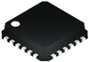
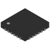
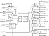
The 8714004I is Zero-Delay Buffer/Frequency Multiplier with eight differential HCSL output pairs, and uses external feedback (differential feedback input and output pairs) for "zero delay" clock regeneration. In PCI Express® and Ethernet applications, 100MHz and 125MHz are the most commonly used reference clock frequencies and each of the eight output pairs can be independently set for either 100MHz or 125MHz. With an output frequency range of 98MHz to 165MHz, the device is also suitable for use in a variety of other applications such as Fibre Channel (106.25MHz) and XAUI (156.25MHz). The M- LVDS Input/Output pair is useful in backplane applications when the reference clock can either be local (on the same board as the 8714004I) or remote via a backplane connector. In output mode, an input from a local reference clock applied to the CLK /nCLK input pins is translated to M- LVDS and driven out to the MLVDS /nMLVDS pins. In input mode, the internal M- LVDS driver is placed in Hi-Z state using the OE_MLVDS pin and MLVDS /nMLVDS pin then becomes an input (e.g. from a backplane). The 8714004I uses very low phase noise FemtoClock technology, thus making it ideal for such applications as PCI Express® Generation 1 and 2 as well as for Gigabit Ethernet, Fibre Channel, and 10 Gigabit Ethernet. It is packaged in a 40- VFQFN package (6mm x 6mm).
Datasheet
Description
The 8714004I is Zero-Delay Buffer/Frequency Multiplier with eight differential HCSL output pairs, and uses external feedback (differential feedback input and output pairs) for "zero delay" clock regeneration. In PCI Express® and Ethernet applications, 100MHz and 125MHz are the most commonly used reference clock frequencies and each of the eight output pairs can be independently set for either 100MHz or 125MHz. With an output frequency range of 98MHz to 165MHz, the device is also suitable for use in a variety of other applications such as Fibre Channel (106.25MHz) and XAUI (156.25MHz). The M- LVDS Input/Output pair is useful in backplane applications when the reference clock can either be local (on the same board as the 8714004I) or remote via a backplane connector. In output mode, an input from a local reference clock applied to the CLK /nCLK input pins is translated to M- LVDS and driven out to the MLVDS /nMLVDS pins. In input mode, the internal M- LVDS driver is placed in Hi-Z state using the OE_MLVDS pin and MLVDS /nMLVDS pin then becomes an input (e.g. from a backplane). The 8714004I uses very low phase noise FemtoClock technology, thus making it ideal for such applications as PCI Express® Generation 1 and 2 as well as for Gigabit Ethernet, Fibre Channel, and 10 Gigabit Ethernet. It is packaged in a 40- VFQFN package (6mm x 6mm).
Datasheet

Suppliers

Company
Product
Description
Supplier Links
FemtoClock Zero Delay Buffer/Clock Generator For PCI Express And Ethernet - 8714004DKILF - Integrated Device Technology
San Jose, CA, USA
FemtoClock Zero Delay Buffer/Clock Generator For PCI Express And Ethernet
8714004DKILF
FemtoClock Zero Delay Buffer/Clock Generator For PCI Express And Ethernet 8714004DKILF
The 8714004I is Zero-Delay Buffer/Frequency Multiplier with eight differential HCSL output pairs, and uses external feedback (differential feedback input and output pairs) for "zero delay" clock regeneration. In PCI Express® and Ethernet applications, 100MHz and 125MHz are the most commonly used reference clock frequencies and each of the eight output pairs can be independently set for either 100MHz or 125MHz. With an output frequency range of 98MHz to 165MHz, the device is also suitable for use in a variety of other applications such as Fibre Channel (106.25MHz) and XAUI (156.25MHz). The M- LVDS Input/Output pair is useful in backplane applications when the reference clock can either be local (on the same board as the 8714004I) or remote via a backplane connector. In output mode, an input from a local reference clock applied to the CLK /nCLK input pins is translated to M- LVDS and driven out to the MLVDS /nMLVDS pins. In input mode, the internal M- LVDS driver is placed in Hi-Z state using the OE_MLVDS pin and MLVDS /nMLVDS pin then becomes an input (e.g. from a backplane). The 8714004I uses very low phase noise FemtoClock technology, thus making it ideal for such applications as PCI Express® Generation 1 and 2 as well as for Gigabit Ethernet, Fibre Channel, and 10 Gigabit Ethernet. It is packaged in a 40- VFQFN package (6mm x 6mm).

The 8714004I is Zero-Delay Buffer/Frequency Multiplier with eight differential HCSL output pairs, and uses external feedback (differential feedback input and output pairs) for "zero delay" clock regeneration. In PCI Express® and Ethernet applications, 100MHz and 125MHz are the most commonly used reference clock frequencies and each of the eight output pairs can be independently set for either 100MHz or 125MHz. With an output frequency range of 98MHz to 165MHz, the device is also suitable for use in a variety of other applications such as Fibre Channel (106.25MHz) and XAUI (156.25MHz). The M- LVDS Input/Output pair is useful in backplane applications when the reference clock can either be local (on the same board as the 8714004I) or remote via a backplane connector. In output mode, an input from a local reference clock applied to the CLK /nCLK input pins is translated to M- LVDS and driven out to the MLVDS /nMLVDS pins. In input mode, the internal M- LVDS driver is placed in Hi-Z state using the OE_MLVDS pin and MLVDS /nMLVDS pin then becomes an input (e.g. from a backplane). The 8714004I uses very low phase noise FemtoClock technology, thus making it ideal for such applications as PCI Express® Generation 1 and 2 as well as for Gigabit Ethernet, Fibre Channel, and 10 Gigabit Ethernet. It is packaged in a 40- VFQFN package (6mm x 6mm).

Supplier's Site Datasheet

Technical Specifications

  Integrated Device Technology
Product Category IC Clocks
Product Number 8714004DKILF
Product Name FemtoClock Zero Delay Buffer/Clock Generator For PCI Express And Ethernet
Device Type Clock Generator
Bus Interface HCSL
Package Type Surface Mount; VFQFPN
Supply Voltage 3.3 volts
Unlock Full Specs
to access all available technical data

Similar Products

CDCE913 Programmable 1-PLL VCXO Clock Synthesizer with 2.5-V or 3.3-V LVCMOS Outputs - CDCE913PW - Texas Instruments
Specs
Package Type TSSOP
Supply Voltage 1.8 volts
Frequency 230 MHz
View Details
9 suppliers
 - 5V9351PFI-G - Rochester Electronics
Rochester Electronics
Specs
Device Type Real Time Clock; Clock Generator
Bus Interface CMOS
Features / Standards RoHS
View Details
Application Specific Clock/Timing - CY28317PVXC-2T-ND - DigiKey
Specs
Device Type Clock Generator
Bus Interface LVCMOS
Package Type Surface Mount; "48-BSSOP (0.295"", 7.50mm Width)"
View Details
4 suppliers
Real Time Clocks - ECS-RTC-3225-5699C3 - ECS Inc. International
Specs
Device Type Real Time Clock
Supply Voltage 2.5 to 5 volts
Operating Temperature -40 to 85 C (-40 to 185 F)
View Details