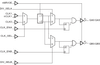

The 87008I is a low skew, 1:8 LVCMOS / LVTTL Clock Generator. The device has 2 banks of 4 outputs and each bank can be independently selected for ÷1 or ÷2 frequency operation. Each bank also has its own power supply pins so that the banks can operate at the following different voltage levels: 3.3V, 2.5V, and 1.8V. The low impedance LVCMOS / LVTTL outputs are designed to drive 50? series or parallel terminated transmission lines. The divide select inputs, DIV_SELA and DIV_SELB, control the output frequency of each bank. The output banks can be independently selected for ÷1 or ÷2 operation. The bank enable inputs, CLK_ENA and CLK_ENB, support enabling and disabling each bank of outputs individually. The CLK_ENA and CLK_ENB circuitry has a synchronizer to prevent runt pulses when enabling or disabling the clock outputs. The master reset input, nMR/ OE , resets the ÷1/÷2 flip flops and also controls the active and high impedance states of all outputs. This pin has an internal pull-up resistor and is normally used only for test purposes or in systems which use low power modes. The 87008I is characterized to operate with the core at 3.3V or 2.5V and the banks at 3.3V, 2.5V, or 1.8V. Guaranteed bank, output, and part-to-part skew characteristics make the 87008I ideal for those clock applications demanding well-defined performance and repeatability.
| Integrated Device Technology | |
|---|---|
| Product Category | IC Clocks |
| Product Number | 87008AGILF |
| Product Name | Low Skew,1-to-8 Differential-to-LVCMOS/LVTTL Clock Generator |
| Device Type | Clock Generator |
| Bus Interface | LVCMOS |
| Package Type | Surface Mount; TSSOP; TSSOP |
| Supply Voltage | 2.5 to 3.3 volts |


