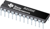
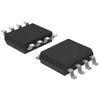
Integrated Device Technology 1:4, Differential-to-LVCMOS / LVTTL Zero Delay Clock Generator 87004AGILF

Description
The 87004I is a highly versatile 1:4 Differential-to- LVCMOS / LVTTL Clock Generator. The 87004I has two selectable clock inputs. The CLK0 , nCLK0 and CLK1 , nCLK1 pairs can accept most standard differential input levels. Internal bias on the nCLK0 and nCLK1 inputs allows the CLK0 and CLK1 inputs to accept LVCMOS / LVTTL . The 87004I has a fully integrated PLL and can be configured as a zero delay buffer, multiplier or divider and has an input and output frequency range of 15.625 MHz to 250 MHz. The reference divider, feedback divider and output divider are each programmable, thereby allowing for the following output-to-input frequency ratios: 8:1, 4:1, 2:1, 1:1, 1:2, 1:4, 1:8. The external feedback allows the device to achieve "zero delay" between the input clock and the output clocks. The PLL_SEL pin can be used to bypass the PLL for system test and debug purposes. In bypass mode, the reference clock is routed around the PLL and into the internal output dividers.
Datasheet
Description
The 87004I is a highly versatile 1:4 Differential-to- LVCMOS / LVTTL Clock Generator. The 87004I has two selectable clock inputs. The CLK0 , nCLK0 and CLK1 , nCLK1 pairs can accept most standard differential input levels. Internal bias on the nCLK0 and nCLK1 inputs allows the CLK0 and CLK1 inputs to accept LVCMOS / LVTTL . The 87004I has a fully integrated PLL and can be configured as a zero delay buffer, multiplier or divider and has an input and output frequency range of 15.625 MHz to 250 MHz. The reference divider, feedback divider and output divider are each programmable, thereby allowing for the following output-to-input frequency ratios: 8:1, 4:1, 2:1, 1:1, 1:2, 1:4, 1:8. The external feedback allows the device to achieve "zero delay" between the input clock and the output clocks. The PLL_SEL pin can be used to bypass the PLL for system test and debug purposes. In bypass mode, the reference clock is routed around the PLL and into the internal output dividers.
Datasheet

Suppliers

Company
Product
Description
Supplier Links
1:4, Differential-to-LVCMOS / LVTTL Zero Delay Clock Generator - 87004AGILF - Integrated Device Technology
San Jose, CA, USA
1:4, Differential-to-LVCMOS / LVTTL Zero Delay Clock Generator
87004AGILF
1:4, Differential-to-LVCMOS / LVTTL Zero Delay Clock Generator 87004AGILF
The 87004I is a highly versatile 1:4 Differential-to- LVCMOS / LVTTL Clock Generator. The 87004I has two selectable clock inputs. The CLK0 , nCLK0 and CLK1 , nCLK1 pairs can accept most standard differential input levels. Internal bias on the nCLK0 and nCLK1 inputs allows the CLK0 and CLK1 inputs to accept LVCMOS / LVTTL . The 87004I has a fully integrated PLL and can be configured as a zero delay buffer, multiplier or divider and has an input and output frequency range of 15.625 MHz to 250 MHz. The reference divider, feedback divider and output divider are each programmable, thereby allowing for the following output-to-input frequency ratios: 8:1, 4:1, 2:1, 1:1, 1:2, 1:4, 1:8. The external feedback allows the device to achieve "zero delay" between the input clock and the output clocks. The PLL_SEL pin can be used to bypass the PLL for system test and debug purposes. In bypass mode, the reference clock is routed around the PLL and into the internal output dividers.

The 87004I is a highly versatile 1:4 Differential-to- LVCMOS / LVTTL Clock Generator. The 87004I has two selectable clock inputs. The CLK0 , nCLK0 and CLK1 , nCLK1 pairs can accept most standard differential input levels. Internal bias on the nCLK0 and nCLK1 inputs allows the CLK0 and CLK1 inputs to accept LVCMOS / LVTTL . The 87004I has a fully integrated PLL and can be configured as a zero delay buffer, multiplier or divider and has an input and output frequency range of 15.625 MHz to 250 MHz. The reference divider, feedback divider and output divider are each programmable, thereby allowing for the following output-to-input frequency ratios: 8:1, 4:1, 2:1, 1:1, 1:2, 1:4, 1:8. The external feedback allows the device to achieve "zero delay" between the input clock and the output clocks. The PLL_SEL pin can be used to bypass the PLL for system test and debug purposes. In bypass mode, the reference clock is routed around the PLL and into the internal output dividers.

Supplier's Site Datasheet

Technical Specifications

  Integrated Device Technology
Product Category IC Clocks
Product Number 87004AGILF
Product Name 1:4, Differential-to-LVCMOS / LVTTL Zero Delay Clock Generator
Device Type Clock Generator
Bus Interface LVCMOS
Package Type Surface Mount; TSSOP; TSSOP
Supply Voltage 2.5 to 3.3 volts
Unlock Full Specs
to access all available technical data

Similar Products

Real Time Clocks - 1897209 - RS Components, Ltd.
RS Components, Ltd.
Specs
Device Type Real Time Clock; Clock Driver
Package Type DIP; Pdip
Operating Temperature 0.0 C (32 F)
View Details
Clock/Timing - Application Specific - AD9575ARUZPEC - Lingto Electronic Limited
Specs
Device Type Clock Generator
Package Type Surface Mount; Surface Mount
Frequency 312 MHz
View Details
Real Time Clocks - 2195-RV-3149-C3-32.768KHZ-OPTION-A-TA-QCTR-ND - DigiKey
Specs
Device Type Real Time Clock
Package Type Surface Mount; 10-VCDFN
Supply Voltage 1.3 to 5.5 volts
View Details
4 suppliers
CDC351 1-Line to 10-Line 3.3V Clock Driver with Tri-State Outputs - CDC351IDWG4 - Texas Instruments
Specs
Device Type Clock Driver
Bus Interface LVTTL
Package Type SOIC,SSOP
View Details
3 suppliers