Integrated Device Technology 2:1 PCIe GEN1/2/3 Clock Multiplexer 5V41068APGGI

Description
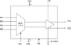
The 5V41068A is a 2:1 differential clock mux for PCI Express applications. It has very low additive jitter making it suitable for use in PCIe Gen2 and Gen3 systems. The 5V41068A selects between 1 of 2 differential HCSL inputs to drive a single differential HCSL output pair. The output can also be terminated to LVDS .
Datasheet
Description
The 5V41068A is a 2:1 differential clock mux for PCI Express applications. It has very low additive jitter making it suitable for use in PCIe Gen2 and Gen3 systems. The 5V41068A selects between 1 of 2 differential HCSL inputs to drive a single differential HCSL output pair. The output can also be terminated to LVDS .
Datasheet

Suppliers

Company
Product
Description
Supplier Links
2:1 PCIe GEN1/2/3 Clock Multiplexer - 5V41068APGGI - Integrated Device Technology
San Jose, CA, USA
2:1 PCIe GEN1/2/3 Clock Multiplexer
5V41068APGGI
2:1 PCIe GEN1/2/3 Clock Multiplexer 5V41068APGGI
The 5V41068A is a 2:1 differential clock mux for PCI Express applications. It has very low additive jitter making it suitable for use in PCIe Gen2 and Gen3 systems. The 5V41068A selects between 1 of 2 differential HCSL inputs to drive a single differential HCSL output pair. The output can also be terminated to LVDS .

The 5V41068A is a 2:1 differential clock mux for PCI Express applications. It has very low additive jitter making it suitable for use in PCIe Gen2 and Gen3 systems. The 5V41068A selects between 1 of 2 differential HCSL inputs to drive a single differential HCSL output pair. The output can also be terminated to LVDS .

Supplier's Site Datasheet

Technical Specifications

  Integrated Device Technology
Product Category Logic Multiplexers
Product Number 5V41068APGGI
Product Name 2:1 PCIe GEN1/2/3 Clock Multiplexer
Supply Voltage 3.3V
Package Type TSSOP; TSSOP 4.4 MM 0.65MM PITCH
Logic Family HCSL,LVDS
Unlock Full Specs
to access all available technical data

Similar Products