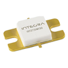
Integra Technologies, Inc. GaN S-Band Radar Transistor IGT2731M130

Description
■ GaN on SiC HEMT Technology ■ POUT-PK = 130W @ 300us/10%/50V ■ 2.7-3.1GHz Instantaneous Operating Frequency Range ■ 50ω Internally Impedance Matched Device ■ Depletion Mode Device ■ Negative Gate Voltage and Bias Sequencing Required ■ Metal Based Package Sealed With Ceramic-Epoxy Lid ■ Gold Metallization System: Chip - Wire Bond - Package ■ Package Size Bolt Down: W=0.800′(20.32mm), L=0.400′(10.16mm) ■ Package Size S(earless): W=0.400′(10.16mm), L=0.400′(10.16mm) ■ 100% High Power RF Tested in Broadband RF Test Fixture
Request a Quote Datasheet
Description
■ GaN on SiC HEMT Technology ■ POUT-PK = 130W @ 300us/10%/50V ■ 2.7-3.1GHz Instantaneous Operating Frequency Range ■ 50ω Internally Impedance Matched Device ■ Depletion Mode Device ■ Negative Gate Voltage and Bias Sequencing Required ■ Metal Based Package Sealed With Ceramic-Epoxy Lid ■ Gold Metallization System: Chip - Wire Bond - Package ■ Package Size Bolt Down: W=0.800′(20.32mm), L=0.400′(10.16mm) ■ Package Size S(earless): W=0.400′(10.16mm), L=0.400′(10.16mm) ■ 100% High Power RF Tested in Broadband RF Test Fixture
Request a Quote Datasheet

Suppliers

Company
Product
Description
Supplier Links
GaN S-Band Radar Transistor - IGT2731M130 - Integra Technologies, Inc.
El Segundo, CA, USA
GaN S-Band Radar Transistor
IGT2731M130
GaN S-Band Radar Transistor IGT2731M130
■ GaN on SiC HEMT Technology ■ POUT-PK = 130W @ 300us/10%/50V ■ 2.7-3.1GHz Instantaneous Operating Frequency Range ■ 50ω Internally Impedance Matched Device ■ Depletion Mode Device ■ Negative Gate Voltage and Bias Sequencing Required ■ Metal Based Package Sealed With Ceramic-Epoxy Lid ■ Gold Metallization System: Chip - Wire Bond - Package ■ Package Size Bolt Down: W=0.800′(20.32mm), L=0.400′(10.16mm) ■ Package Size S(earless): W=0.400′(10.16mm), L=0.400′(10.16mm) ■ 100% High Power RF Tested in Broadband RF Test Fixture

■ GaN on SiC HEMT Technology
■ POUT-PK = 130W @ 300us/10%/50V
■ 2.7-3.1GHz Instantaneous Operating Frequency Range
■ 50Ω Internally Impedance Matched Device
■ Depletion Mode Device
■ Negative Gate Voltage and Bias Sequencing Required
■ Metal Based Package Sealed With Ceramic-Epoxy Lid
■ Gold Metallization System: Chip - Wire Bond - Package
■ Package Size Bolt Down: W=0.800″(20.32mm), L=0.400″(10.16mm)
■ Package Size S(earless): W=0.400″(10.16mm), L=0.400″(10.16mm)
■ 100% High Power RF Tested in Broadband RF Test Fixture

Supplier's Site
RF FETs, MOSFETs - 2251-IGT2731M130-ND - DigiKey
Thief River Falls, MN, United States
RF FETs, MOSFETs
2251-IGT2731M130-ND
RF FETs, MOSFETs 2251-IGT2731M130-ND
RF Mosfet

RF Mosfet

Buy Now Datasheet

Technical Specifications

  Integra Technologies, Inc. DigiKey
Product Category RF MOSFET Transistors Transistors
Product Number IGT2731M130 2251-IGT2731M130-ND
Product Name GaN S-Band Radar Transistor RF FETs, MOSFETs
Transistor Technology / Material GaN
Unlock Full Specs
to access all available technical data
