High-efficiency OptiMOS™ 70 A integrated power stage with internal current sense
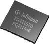
Infineon’s TDA21570, 70 A integrated power stage, contains a low quiescent current synchronous buck gate-driver IC. In addition, the TDA21570 combines control and synchronous MOSFETs along with an active diode structure that achieves low VSD similar to a Schottky Diode with very little reverse recovery charge.
The package is optimized for PCB layout, heat transfer, driver/MOSFET control timing, and minimal switch node ringing when layout guidelines are followed. The paired gate driver and MOSFET combination enables higher efficiency at lower output voltages required by cutting edge CPU, GPU and DDR memory designs.
Operation of up to 1.5 MHz switching frequency enables high performance transient response, allowing miniaturization of output inductors, as well as input and output capacitors while maintaining industry leading efficiency.
Summary of Features
Integrated driver, active diode, control MOSFET Q1 and synchronous MOSFET Q2
On-chip MOSFET current sensing and reporting at 5 µA/A
Input voltage (VIN) range of 4.25 V to 16 V
Output current capability of 70 A
Enhanced Fault reporting and identification
Over temperature protection and thermal shutdown
Auto-replenishment on bootstrap capacitor
Compatible with 3.3 V tri-state PWM Input
DEEP SLEEP mode for power saving via EN= low (32 µA typ)
Small 5 mm x 6 mm x 0.9 mm PQFN package
Benefits
High efficiency
Industry best current sense accuracy
Enhance fault identification and reporting
Advanced protection features like high-side MOSFET short detection, over temp and thermal shutdown
Low quiescent for power saving via EN = low
Potential Applications
High frequency, low profile DC-DC converters
Voltage regulators for CPUs, GPUs and DDR memory arrays
Telecom controlled and uncontrolled
Applications
48 V intermediate bus converter (IBC)
Edge computing
Industrial PC
Programmable logic controller (PLC)
Telecommunication infrastructure
Designers who used this product also designed with
BSC014N04LSI | N-Channel Power MOSFET
BSC032N04LS | N-Channel Power MOSFET
XDPE14284A-0000 | Digital Multiphase Controllers
IPB017N10N5LF | N-Channel Power MOSFET
IR3889MTRPBF | Integrated POL Voltage Regulators
BSS214N | Small signal/small power MOSFET
SLB 9670VQ2.0 | OPTIGA™ TPM - Trusted Platform Module
BSC014N04LSI | N-Channel Power MOSFET
BSC032N04LS | N-Channel Power MOSFET
XDPE14284A-0000 | Digital Multiphase Controllers
IPB017N10N5LF | N-Channel Power MOSFET
IR3889MTRPBF | Integrated POL Voltage Regulators
BSS214N | Small signal/small power MOSFET
SLB 9670VQ2.0 | OPTIGA™ TPM - Trusted Platform Module
BSC014N04LSI | N-Channel Power MOSFET
1 2
High-efficiency OptiMOS™ 70 A integrated power stage with internal current sense
Infineon’s TDA21570, 70 A integrated power stage, contains a low quiescent current synchronous buck gate-driver IC. In addition, the TDA21570 combines control and synchronous MOSFETs along with an active diode structure that achieves low VSD similar to a Schottky Diode with very little reverse recovery charge.
The package is optimized for PCB layout, heat transfer, driver/MOSFET control timing, and minimal switch node ringing when layout guidelines are followed. The paired gate driver and MOSFET combination enables higher efficiency at lower output voltages required by cutting edge CPU, GPU and DDR memory designs.
Operation of up to 1.5 MHz switching frequency enables high performance transient response, allowing miniaturization of output inductors, as well as input and output capacitors while maintaining industry leading efficiency.
Summary of Features
- Integrated driver, active diode, control MOSFET Q1 and synchronous MOSFET Q2
- On-chip MOSFET current sensing and reporting at 5 µA/A
- Input voltage (VIN) range of 4.25 V to 16 V
- Output current capability of 70 A
- Enhanced Fault reporting and identification
- Over temperature protection and thermal shutdown
- Auto-replenishment on bootstrap capacitor
- Compatible with 3.3 V tri-state PWM Input
- DEEP SLEEP mode for power saving via EN= low (32 µA typ)
- Small 5 mm x 6 mm x 0.9 mm PQFN package
Benefits
- High efficiency
- Industry best current sense accuracy
- Enhance fault identification and reporting
- Advanced protection features like high-side MOSFET short detection, over temp and thermal shutdown
- Low quiescent for power saving via EN = low
Potential Applications
- High frequency, low profile DC-DC converters
- Voltage regulators for CPUs, GPUs and DDR memory arrays
- Telecom controlled and uncontrolled
Applications
- 48 V intermediate bus converter (IBC)
- Edge computing
- Industrial PC
- Programmable logic controller (PLC)
- Telecommunication infrastructure
Designers who used this product also designed with
- BSC014N04LSI |
N-Channel Power MOSFET
- BSC032N04LS |
N-Channel Power MOSFET
- XDPE14284A-0000 |
Digital Multiphase Controllers
- IPB017N10N5LF |
N-Channel Power MOSFET
- IR3889MTRPBF |
Integrated POL Voltage Regulators
- BSS214N |
Small signal/small power MOSFET
- SLB 9670VQ2.0 |
OPTIGA™ TPM - Trusted Platform Module
- BSC014N04LSI |
N-Channel Power MOSFET
- BSC032N04LS |
N-Channel Power MOSFET
- XDPE14284A-0000 |
Digital Multiphase Controllers
- IPB017N10N5LF |
N-Channel Power MOSFET
- IR3889MTRPBF |
Integrated POL Voltage Regulators
- BSS214N |
Small signal/small power MOSFET
- SLB 9670VQ2.0 |
OPTIGA™ TPM - Trusted Platform Module
- BSC014N04LSI |
N-Channel Power MOSFET
1
2