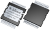
650 V CoolMOS™ CFD7A N-channel automotive SJ power MOSFET in HDSOP-22 top-side cooling
The 60mΩ IPDQ65R060CFD7A in QDPAK top side cooling SMD package is part of the automotive-qualified 650 V CoolMOS™ SJ power MOSFET CFD7A product family. As compared to the previous generation, CoolMOS™ CFD7A offers higher reliability and power density while increasing design flexibility. Top side cooling further supports increased power density, reduces parasitic source inductance and comes with Kelvin source pin and 3.2 mm creepage distance.
Summary of Features
AEC-Q101 qualified
For hard- and soft-switching topologies
Intrinsic fast body diode
Reduced parasitic source inductance
Kelvin source pin
High current capability
High power dissipation, Ptot 694 W/25°C
Creepage distance of 3.2 mm for HV
Benefits
Better utilization of PCB space
Highest reliability for automotive appl.
Optimized power loop
Decoupling of thermals from substrate
Enabling of higher power density designs
Scalable for use in PFC and DC-DC stage
Granular portfolio available
Potential Applications
On-board chargers
HV-LV DC-DC converters
Auxiliary power supplies
Applications
AC-DC auxiliary power supplies
High-voltage DC-DC converter for electric vehicles
On-board charging (OBC) for electric vehicles
650 V CoolMOS™ CFD7A N-channel automotive SJ power MOSFET in HDSOP-22 top-side cooling
The 60mΩ IPDQ65R060CFD7A in QDPAK top side cooling SMD package is part of the automotive-qualified 650 V CoolMOS™ SJ power MOSFET CFD7A product family. As compared to the previous generation, CoolMOS™ CFD7A offers higher reliability and power density while increasing design flexibility. Top side cooling further supports increased power density, reduces parasitic source inductance and comes with Kelvin source pin and
3.2 mm creepage distance.
Summary of Features
- AEC-Q101 qualified
- For hard- and soft-switching topologies
- Intrinsic fast body diode
- Reduced parasitic source inductance
- Kelvin source pin
- High current capability
- High power dissipation, Ptot 694 W/25°C
- Creepage distance of 3.2 mm for HV
Benefits
- Better utilization of PCB space
- Highest reliability for automotive appl.
- Optimized power loop
- Decoupling of thermals from substrate
- Enabling of higher power density designs
- Scalable for use in PFC and DC-DC stage
- Granular portfolio available
Potential Applications
- On-board chargers
- HV-LV DC-DC converters
- Auxiliary power supplies
Applications
- AC-DC auxiliary power supplies
- High-voltage DC-DC converter for electric vehicles
- On-board charging (OBC) for electric vehicles