Infineon Technologies AG RF - Antenna tuners - BGSA402ML10 BGSA402ML10

Description
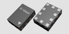
The BGSA402ML10 is a versatile shunt to ground 4xSingle-Pole Single-Throw (4xSPST) RF antenna tuning switch. It is optimized for low COFF as well as low RON enabling applications up to 6 GHz. The BGSA402ML10 is ideal for antenna tuning application. This chip integrates on-chip CMOS logic and power supply regulation. Its digital control interface is compliant with MIPI2.1 RFFE specification and each switch throw can be programmed individually or all together in the same RFFE command frame. Up to 2 instantiations of the same device can be controlled using the same RFFE bus thanks to its 2 states USID_Sel pin. Unlike GaAs technology, the 0.1 dB compression point exceeds the switch maximum input power level, resulting in excellent linear performance at all signal levels within the operating conditions. External DC blocking capacitors at the RF ports are only required if DC voltage is applied externally. Due to its high RF voltage ruggedness, it is suited for switching any reactive device such as inductor and capacitor in RF matching circuits without significant losses. Summary of Features Designed for high-linearity antenna aperture switching and RF tuning applications Multiple selectable switch configurations Ultra low RON resistance of 1.49 in ON state Low COFF capacitance of 170 fF in OFF state High RF operating voltage OFF state handling of >45 V Low harmonic generation MIPI RFFE 2.1 compliant control interface Support 2 default USID via USID_Sel pin state Supply voltage range: 1.65 to 3.6 V No RF parameter change within supply voltage range Small form factor 1.1 mm x 1.5 mm, MSL1, 260 C per JEDEC J-STD-020 RoHS and WEEE compliant package Potential Applications Impedance tuning Antenna tuning Inductance tuning Tunable filters
Request a Quote Datasheet
Description
The BGSA402ML10 is a versatile shunt to ground 4xSingle-Pole Single-Throw (4xSPST) RF antenna tuning switch. It is optimized for low COFF as well as low RON enabling applications up to 6 GHz. The BGSA402ML10 is ideal for antenna tuning application. This chip integrates on-chip CMOS logic and power supply regulation. Its digital control interface is compliant with MIPI2.1 RFFE specification and each switch throw can be programmed individually or all together in the same RFFE command frame. Up to 2 instantiations of the same device can be controlled using the same RFFE bus thanks to its 2 states USID_Sel pin. Unlike GaAs technology, the 0.1 dB compression point exceeds the switch maximum input power level, resulting in excellent linear performance at all signal levels within the operating conditions. External DC blocking capacitors at the RF ports are only required if DC voltage is applied externally. Due to its high RF voltage ruggedness, it is suited for switching any reactive device such as inductor and capacitor in RF matching circuits without significant losses. Summary of Features Designed for high-linearity antenna aperture switching and RF tuning applications Multiple selectable switch configurations Ultra low RON resistance of 1.49 in ON state Low COFF capacitance of 170 fF in OFF state High RF operating voltage OFF state handling of >45 V Low harmonic generation MIPI RFFE 2.1 compliant control interface Support 2 default USID via USID_Sel pin state Supply voltage range: 1.65 to 3.6 V No RF parameter change within supply voltage range Small form factor 1.1 mm x 1.5 mm, MSL1, 260 C per JEDEC J-STD-020 RoHS and WEEE compliant package Potential Applications Impedance tuning Antenna tuning Inductance tuning Tunable filters
Request a Quote Datasheet

Suppliers

Company
Product
Description
Supplier Links
RF - Antenna tuners - BGSA402ML10 - BGSA402ML10 - Infineon Technologies AG
Neubiberg, Germany
RF - Antenna tuners - BGSA402ML10
BGSA402ML10
RF - Antenna tuners - BGSA402ML10 BGSA402ML10
The BGSA402ML10 is a versatile shunt to ground 4xSingle-Pole Single-Throw (4xSPST) RF antenna tuning switch. It is optimized for low COFF as well as low RON enabling applications up to 6 GHz. The BGSA402ML10 is ideal for antenna tuning application. This chip integrates on-chip CMOS logic and power supply regulation. Its digital control interface is compliant with MIPI2.1 RFFE specification and each switch throw can be programmed individually or all together in the same RFFE command frame. Up to 2 instantiations of the same device can be controlled using the same RFFE bus thanks to its 2 states USID_Sel pin. Unlike GaAs technology, the 0.1 dB compression point exceeds the switch maximum input power level, resulting in excellent linear performance at all signal levels within the operating conditions. External DC blocking capacitors at the RF ports are only required if DC voltage is applied externally. Due to its high RF voltage ruggedness, it is suited for switching any reactive device such as inductor and capacitor in RF matching circuits without significant losses. Summary of Features Designed for high-linearity antenna aperture switching and RF tuning applications Multiple selectable switch configurations Ultra low RON resistance of 1.49 in ON state Low COFF capacitance of 170 fF in OFF state High RF operating voltage OFF state handling of >45 V Low harmonic generation MIPI RFFE 2.1 compliant control interface Support 2 default USID via USID_Sel pin state Supply voltage range: 1.65 to 3.6 V No RF parameter change within supply voltage range Small form factor 1.1 mm x 1.5 mm, MSL1, 260 C per JEDEC J-STD-020 RoHS and WEEE compliant package Potential Applications Impedance tuning Antenna tuning Inductance tuning Tunable filters

The BGSA402ML10 is a versatile shunt to ground 4xSingle-Pole Single-Throw (4xSPST) RF antenna tuning switch. It is optimized for low COFF as well as low RON enabling applications up to 6 GHz.

The BGSA402ML10 is ideal for antenna tuning application. This chip integrates on-chip CMOS logic and power supply regulation. Its digital control interface is compliant with MIPI2.1 RFFE specification and each switch throw can be programmed individually or all together in the same RFFE command frame. Up to 2 instantiations of the same device can be controlled using the same RFFE bus thanks to its 2 states USID_Sel pin.

Unlike GaAs technology, the 0.1 dB compression point exceeds the switch maximum input power level, resulting in excellent linear performance at all signal levels within the operating conditions. External DC blocking capacitors at the RF ports are only required if DC voltage is applied externally. Due to its high RF voltage ruggedness, it is suited for switching any reactive device such as inductor and capacitor in RF matching circuits without significant losses.


Summary of Features

  • Designed for high-linearity antenna aperture switching and RF tuning applications
  • Multiple selectable switch configurations
  • Ultra low RON resistance of 1.49 in ON state
  • Low COFF capacitance of 170 fF in OFF state
  • High RF operating voltage OFF state handling of >45 V
  • Low harmonic generation
  • MIPI RFFE 2.1 compliant control interface
  • Support 2 default USID via USID_Sel pin state
  • Supply voltage range: 1.65 to 3.6 V
  • No RF parameter change within supply voltage range
  • Small form factor 1.1 mm x 1.5 mm, MSL1, 260 C per JEDEC J-STD-020
  • RoHS and WEEE compliant package

Potential Applications

  • Impedance tuning
  • Antenna tuning
  • Inductance tuning
  • Tunable filters
Supplier's Site Datasheet

Technical Specifications

  Infineon Technologies AG
Product Category RF Switches
Product Number BGSA402ML10
Product Name RF - Antenna tuners - BGSA402ML10
Control Interface MIPI
Unlock Full Specs
to access all available technical data

Similar Products

RF ICs - 2224776P - RS Components, Ltd.
Infineon Technologies AG
Specs
Package Type TSLP
View Details
5 suppliers
RF Switches - BGSF18DM20E6327XUMA1138 - Quarktwin Technology Ltd.
View Details
2 suppliers
 - BGS13GA14E6327XTSA1 - Rochester Electronics
Infineon Technologies AG
View Details
3 suppliers
RF Switches - BGS12AL74E6327XTSA1TR-ND - DigiKey
Infineon Technologies AG
Specs
Package Type Surface Mount; 6-XFDFN Exposed Pad
Operating Temperature -30 to 85 C (-22 to 185 F)
Frequency Range 30 to 3000 MHz
View Details
3 suppliers