Fischer Technology, Inc. EDXRF Instrument for Non-destructive Microstructure Wafer Metrology FISCHERSCOPE® X-RAY XDV®-µ SEMI

Description
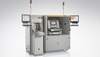
The FISCHERSCOPE X-RAY XDV-μ SEMI is an automated measurement system optimized for the quality control of micro-structures in complex 2.5D/3D packaging applications in the semiconductor industry. Fully automated analysis prevents damage to valuable wafer material. And consistent test conditions deliver reliable results. The instrument is suitable for use in clean rooms, and a comprehensive equipment catalog allows simple integration into existing wafer fabs. Features: Fully automated wafer handling and test process enables efficient staff deployment Can precisely test structures up to 10 µm in diameter Automatically locates positions to be measured with image recognition Simple operation via Fischer WinFTM software Individually applicable: manual measurements are possible at any time Flexible: docking station for FOUP, SMIF and cassette, for 6"", 8"" and 12"" wafers Applications: Coating Thickness Measurement Base metallization layers (UBM) on a nanometer scale Thin lead-free solder caps on copper pillars Extremely small contact surfaces and other complex 2.5D/3D packaging applications Material Analysis C4 and smaller solder bumps Lead-free solder caps on copper pillars
Datasheet
Description
The FISCHERSCOPE X-RAY XDV-μ SEMI is an automated measurement system optimized for the quality control of micro-structures in complex 2.5D/3D packaging applications in the semiconductor industry. Fully automated analysis prevents damage to valuable wafer material. And consistent test conditions deliver reliable results. The instrument is suitable for use in clean rooms, and a comprehensive equipment catalog allows simple integration into existing wafer fabs. Features: Fully automated wafer handling and test process enables efficient staff deployment Can precisely test structures up to 10 µm in diameter Automatically locates positions to be measured with image recognition Simple operation via Fischer WinFTM software Individually applicable: manual measurements are possible at any time Flexible: docking station for FOUP, SMIF and cassette, for 6"", 8"" and 12"" wafers Applications: Coating Thickness Measurement Base metallization layers (UBM) on a nanometer scale Thin lead-free solder caps on copper pillars Extremely small contact surfaces and other complex 2.5D/3D packaging applications Material Analysis C4 and smaller solder bumps Lead-free solder caps on copper pillars
Datasheet

Suppliers

Company
Product
Description
Supplier Links
EDXRF Instrument for Non-destructive Microstructure Wafer Metrology - FISCHERSCOPE® X-RAY XDV®-µ SEMI - Fischer Technology, Inc.
Windsor, CT, USA
EDXRF Instrument for Non-destructive Microstructure Wafer Metrology
FISCHERSCOPE® X-RAY XDV®-µ SEMI
EDXRF Instrument for Non-destructive Microstructure Wafer Metrology FISCHERSCOPE® X-RAY XDV®-µ SEMI
The FISCHERSCOPE X-RAY XDV-μ SEMI is an automated measurement system optimized for the quality control of micro-structures in complex 2.5D/3D packaging applications in the semiconductor industry. Fully automated analysis prevents damage to valuable wafer material. And consistent test conditions deliver reliable results. The instrument is suitable for use in clean rooms, and a comprehensive equipment catalog allows simple integration into existing wafer fabs. Features: Fully automated wafer handling and test process enables efficient staff deployment Can precisely test structures up to 10 µm in diameter Automatically locates positions to be measured with image recognition Simple operation via Fischer WinFTM software Individually applicable: manual measurements are possible at any time Flexible: docking station for FOUP, SMIF and cassette, for 6"", 8"" and 12"" wafers Applications: Coating Thickness Measurement Base metallization layers (UBM) on a nanometer scale Thin lead-free solder caps on copper pillars Extremely small contact surfaces and other complex 2.5D/3D packaging applications Material Analysis C4 and smaller solder bumps Lead-free solder caps on copper pillars
The FISCHERSCOPE X-RAY XDV-μ SEMI is an automated measurement system optimized for the quality control of micro-structures in complex 2.5D/3D packaging applications in the semiconductor industry. Fully automated analysis prevents damage to valuable wafer material. And consistent test conditions deliver reliable results. The instrument is suitable for use in clean rooms, and a comprehensive equipment catalog allows simple integration into existing wafer fabs.

Features:

  • Fully automated wafer handling and test process enables efficient staff deployment
  • Can precisely test structures up to 10 µm in diameter
  • Automatically locates positions to be measured with image recognition
  • Simple operation via Fischer WinFTM software
  • Individually applicable: manual measurements are possible at any time
  • Flexible: docking station for FOUP, SMIF and cassette, for 6"", 8"" and 12"" wafers

Applications:

Coating Thickness Measurement

  • Base metallization layers (UBM) on a nanometer scale
  • Thin lead-free solder caps on copper pillars
  • Extremely small contact surfaces and other complex 2.5D/3D packaging applications

Material Analysis

  • C4 and smaller solder bumps
  • Lead-free solder caps on copper pillars
Supplier's Site Datasheet

Technical Specifications

  Fischer Technology, Inc.
Product Category Dimensional Gages and Instruments
Product Number FISCHERSCOPE® X-RAY XDV®-µ SEMI
Product Name EDXRF Instrument for Non-destructive Microstructure Wafer Metrology
Mounting / Loading Options Benchtop or Floor
Unlock Full Specs
to access all available technical data

Similar Products

Optical thickness gauge for heavy plate mills - thicknessCONTROL MTS 9201.LLT-60/2500 - Micro-Epsilon Group
Specs
Mounting / Loading Options Machine Mounted; Automatic or Inline
Measurement Scale / Units English; Metric
Gage / Instrument Type Laser micrometer; Gage Set or Tool Kit; Laser line triangulation
View Details
Thickness measurement system - C11295 - Hamamatsu Photonics Europe
Hamamatsu Photonics Europe
Specs
Measurement Scale / Units Metric
Gaging Technology Optical
Attribute Measurement Capability Thickness Gage
View Details
UT343E Coating Thickness Gauge - Professional Grade - UT343E - Uni-Trend US
Specs
Attribute Measurement Capability Thickness Gage
View Details
Micrometer Head, Standard Resolution, 40 mm Travel, 100 lb. Load - BM25.40 - Newport MKS
Specs
Mounting / Loading Options M18x1.0
Measurement Scale / Units Metric
Gage / Instrument Type Micrometer
View Details