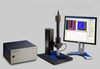
High-Resolution Film Thickness Maps
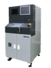
The Filmetrics F42 can map the thickness of films, such as OSP, at over one-million points, each with a spot size as small as 3 microns. Using an integrated CCD camera, live video makes it easy to pinpoint exact measurement locations. Once the feature is in the field of view, simply draw a box around it to analyze it.
Pixel-Width Spot Size
Thickness measurement is made at every single pixel displayed, yielding spot sizes as small as 3 microns. This allows measurements to be made in even the narrowest of channels and cavities.
Mapping
Uniformity can be checked on these structures with the F42 system's mapping capability. With one click, over a million individual thicknesses can be calculated and displayed in an easy-to-read gradient map. Average thickness and other statistics are automatically reported while notifying the user of any out-of-range thickness measurements. Using goodness-of-fit criteria, the features of interest can be mapped while excluding all other areas.
Common Applications:
OSP on Printed Circuit Boards
Semiconductor Fabrication
Liquid Crystal and OLED Displays
What's Included
Measurement Stage with motorized focus and standard 5x objective lens
Integrated Light Source/Control Unit
FILMeasure 7.0 software
BK-7 reference material
TS-Focus-SiO2-4-1000
0 Focus/Thickness standard
FILMeasure standalone software for remote data analysis
Tweezers
High-Resolution Film Thickness Maps
The Filmetrics F42 can map the thickness of films, such as OSP, at over one-million points, each with a spot size as small as 3 microns. Using an integrated CCD camera, live video makes it easy to pinpoint exact measurement locations. Once the feature is in the field of view, simply draw a box around it to analyze it.
Pixel-Width Spot Size
Thickness measurement is made at every single pixel displayed, yielding spot sizes as small as 3 microns. This allows measurements to be made in even the narrowest of channels and cavities.
Mapping
Uniformity can be checked on these structures with the F42 system's mapping capability. With one click, over a million individual thicknesses can be calculated and displayed in an easy-to-read gradient map. Average thickness and other statistics are automatically reported while notifying the user of any out-of-range thickness measurements. Using goodness-of-fit criteria, the features of interest can be mapped while excluding all other areas.
Common Applications:
- OSP on Printed Circuit Boards
- Semiconductor Fabrication
- Liquid Crystal and OLED Displays
What's Included
- Measurement Stage with motorized focus and standard 5x objective lens
- Integrated Light Source/Control Unit
- FILMeasure 7.0 software
- BK-7 reference material
- TS-Focus-SiO2-4-10000 Focus/Thickness standard
- FILMeasure standalone software for remote data analysis
- Tweezers