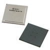
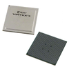
Advanced Micro Devices, Inc. Embedded - FPGAs (Field Programmable Gate Array) XC2VP50-6FFG1148C

Description
IC FPGA 812 I/O 1148FCBGA
Description
IC FPGA 812 I/O 1148FCBGA
Datasheet
Datasheet Summary
Powered by GS/AI

The XC2VP50-6FFG1148C is a member of the Virtex-II Pro FPGA family, designed for high-performance applications. It features up to 53,136 logic cells and supports a maximum of 4,176 user I/O pads. The device includes two embedded IBM PowerPC RISC processor blocks and can accommodate up to 16 RocketIO multi-gigabit transceivers, enabling high-speed serial communication with baud rates ranging from 600 Mb/s to 3.125 Gb/s. This FPGA utilizes SRAM-based in-system configuration and offers a flexible logic architecture with dedicated 18-bit x 18-bit multiplier blocks and a comprehensive memory hierarchy, including SelectRAM+ resources. The device is equipped with advanced clock management capabilities, including multiple Digital Clock Managers (DCMs) for precise clock de-skewing and frequency synthesis. The XC2VP50-6FFG1148C is suitable for applications requiring high data throughput and complex processing capabilities, making it a viable option for engineers looking for a robust FPGA solution in demanding environments.

Datasheet Summary
Powered by GS/AI

The XC2VP50-6FFG1148C is a member of the Virtex-II Pro FPGA family, designed for high-performance applications. It features up to 53,136 logic cells and supports a maximum of 4,176 user I/O pads. The device includes two embedded IBM PowerPC RISC processor blocks and can accommodate up to 16 RocketIO multi-gigabit transceivers, enabling high-speed serial communication with baud rates ranging from 600 Mb/s to 3.125 Gb/s. This FPGA utilizes SRAM-based in-system configuration and offers a flexible logic architecture with dedicated 18-bit x 18-bit multiplier blocks and a comprehensive memory hierarchy, including SelectRAM+ resources. The device is equipped with advanced clock management capabilities, including multiple Digital Clock Managers (DCMs) for precise clock de-skewing and frequency synthesis. The XC2VP50-6FFG1148C is suitable for applications requiring high data throughput and complex processing capabilities, making it a viable option for engineers looking for a robust FPGA solution in demanding environments.

Suppliers

Company
Product
Description
Supplier Links
Embedded - FPGAs (Field Programmable Gate Array) - XC2VP50-6FFG1148C - Lingto Electronic Limited
Shenzhen, China
Embedded - FPGAs (Field Programmable Gate Array)
XC2VP50-6FFG1148C
Embedded - FPGAs (Field Programmable Gate Array) XC2VP50-6FFG1148C
IC FPGA 812 I/O 1148FCBGA

IC FPGA 812 I/O 1148FCBGA

Supplier's Site Datasheet
FPGAs (Field Programmable Gate Array) - XC2VP50-6FFG1148C - Quarktwin Technology Ltd.
Shenzhen, Guangdong, China
FPGAs (Field Programmable Gate Array)
XC2VP50-6FFG1148C
FPGAs (Field Programmable Gate Array) XC2VP50-6FFG1148C
Virtex®-II Pro Field Programmable Gate Array (FPGA) IC 812 4276224 53136 1148-BBGA, FCBGA

Virtex®-II Pro Field Programmable Gate Array (FPGA) IC 812 4276224 53136 1148-BBGA, FCBGA

Buy Now Datasheet
FPGAs (Field Programmable Gate Array) - XC2VP50-6FFG1148C - Quarktwin Technology Ltd.
Shenzhen, Guangdong, China
FPGAs (Field Programmable Gate Array)
XC2VP50-6FFG1148C
FPGAs (Field Programmable Gate Array) XC2VP50-6FFG1148C
Virtex®-II Pro Field Programmable Gate Array (FPGA) IC 812 4276224 53136 1148-BBGA, FCBGA

Virtex®-II Pro Field Programmable Gate Array (FPGA) IC 812 4276224 53136 1148-BBGA, FCBGA

Buy Now Datasheet

Technical Specifications

  Lingto Electronic Limited Quarktwin Technology Ltd.
Product Category Field-Programmable Gate Arrays (FPGA) Field-Programmable Gate Arrays (FPGA)
Product Number XC2VP50-6FFG1148C XC2VP50-6FFG1148C
Product Name Embedded - FPGAs (Field Programmable Gate Array) FPGAs (Field Programmable Gate Array)
Logic Cells / Logic Blocks 53136 53136
User I/Os 812 pins 812 pins
Package Type Other; 1148-BBGA, FCBGA
Unlock Full Specs
to access all available technical data