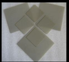
Rubicon’s sapphire epi-polished wafers are ultra-flat, super clean, stress-free large diameter substrates, offered with precision orientations and offsets and wafer-to-wafer uniformity, with one or both surfaces finished. These sapphire wafers are custom designed to meet customers’ unique specifications for final application.
Material
ES2 High Purity Sapphire (99.999%)
Bubble/Color
None by visual inspection under high intensity light
Grain Boundary/Lineage
None by visual inspection under Lineage polarized light
Orientation
C–Plane (0001)
A–Plane (11-20)
R–Plane (10-12)
M–Plane (10-10)
Random
Orientation Tilt Tolerance
Customer Preference
up to 6” ±0.05
up to 8” ±0.10
Diameter
Up to 200 mm
Flatness (Focal Plane Deviation)
Up to 6” ≤4.0 μm
Up to 8” ≤6.0 μm
BOW
Up to 6” 0 ± 15 μm
Up to 8” 0 ± 20 μm
WARP
Up to 6” ≤30 μm
Up to 8” ≤40 μm
TTV
Up to 8” ≤20 μm
Thickness Tolerance
Customer Preference
± 25 μm
Surface Finish
Up to Ra ≤ 0.2 nm for front side
Up to Ra ≤ 1 μm for back side
Orientation Flat/Notch
SEMI/JEITA standard
Edge Bevel
Industry Standard
Cleanliness
Surface to be free from all visual contaminants
Packaging
Vacuum-sealed containers with nitrogen backfill in a class 100 environment
Available Options
Laser Marking
Optical Polished Finish
Single Side Epi Ready Finish
Double Side Epi Ready Finish
Rubicon’s sapphire epi-polished wafers are ultra-flat, super clean, stress-free large diameter substrates, offered with precision orientations and offsets and wafer-to-wafer uniformity, with one or both surfaces finished. These sapphire wafers are custom designed to meet customers’ unique specifications for final application.
Material
- ES2 High Purity Sapphire (99.999%)
Bubble/Color
- None by visual inspection under high
intensity light
Grain Boundary/Lineage
- None by visual inspection under Lineage polarized light
Orientation
- C–Plane (0001)
- A–Plane (11-20)
- R–Plane (10-12)
- M–Plane (10-10)
- Random
Orientation Tilt Tolerance
- Customer Preference
- up to 6” ±0.05
- up to 8” ±0.10
Diameter
Flatness (Focal Plane Deviation)
- Up to 6” ≤4.0 μm
- Up to 8” ≤6.0 μm
BOW
- Up to 6” 0 ± 15 μm
- Up to 8” 0 ± 20 μm
WARP
- Up to 6” ≤30 μm
- Up to 8” ≤40 μm
TTV
Thickness Tolerance
- Customer Preference
- ± 25 μm
Surface Finish
- Up to Ra ≤ 0.2 nm for front side
- Up to Ra ≤ 1 μm for back side
Orientation Flat/Notch
Edge Bevel
Cleanliness
- Surface to be free from all visual contaminants
Packaging
- Vacuum-sealed containers with nitrogen backfill in a class 100 environment
Available Options
- Laser Marking
- Optical Polished Finish
- Single Side Epi Ready Finish
- Double Side Epi Ready Finish