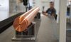
Due to its high electrical conductivity, copper is becoming increasingly popular for use in large-format, high-resolution TFT-LCD television sets. Copper is used as the electrode layer in thin-film transistors. The copper layer controls the individual image dots (pixels) and therefore determines the quality of the obtained image.
Totally pure.
Impurities in the sputtering targets impair the electrical conductivity of the material. Impurities in the form of titanium, phosphorous, calcium, iron, chromium and selenium are particularly critical. These metals are present in tiny quantities in our copper targets. They are present only in concentrations well below the critical threshold values.
Maximum density.
Our special production processes allow for our copper sputtering targets to have a density of nearly 100 %. As a result, your process benefits from a particularly high level of conductivity and time savings due to the excellent sputtering speeds.
Well structured.
Our copper targets have a particularly fine-grained microstructure. This ensures that you benefit from uniform erosion and a low susceptibility to particle formation throughout the sputtering process.
One-step Mo/Cu wet etching.
In electrode layers, copper is mostly used in combination with a molybdenum adhesion promotion layer/diffusion barrier. To structure the Mo-Cu multilayers, we have worked together with the Korean Aerospace University and leading chemicals manufacturers to develop a new etching process.
The benefits to you:
Contains no hydrogen peroxide
Environmentally friendly and non-explosive
Suitable for use in standard aluminum etching equipment
You want the perfect coating? We create it.
In the PVD process, everything must fit together perfectly. Only if all the process parameters are fully harmonized it is possible to create the coating that precisely meets your requirements. In our PVD application laboratory, we perform sputtering in near-real life conditions. Here, our team of developers creates coatings and conducts in-depth analyses based on your specifications. Thanks to this collaboration with you and a wide range of development institutes, we can minimize the time to market required for the development of new coating materials.
The best proof of our expertise is us! We coat many of our products such as semiconductor base plates and x-ray targets in-house using the PVD, CVD, APS and VPS coating processes.
Due to its high electrical conductivity, copper is becoming increasingly popular for use in large-format, high-resolution TFT-LCD television sets. Copper is used as the electrode layer in thin-film transistors. The copper layer controls the individual image dots (pixels) and therefore determines the quality of the obtained image.
Totally pure.
Impurities in the sputtering targets impair the electrical conductivity of the material. Impurities in the form of titanium, phosphorous, calcium, iron, chromium and selenium are particularly critical. These metals are present in tiny quantities in our copper targets. They are present only in concentrations well below the critical threshold values.
Maximum density.
Our special production processes allow for our copper sputtering targets to have a density of nearly 100 %. As a result, your process benefits from a particularly high level of conductivity and time savings due to the excellent sputtering speeds.
Well structured.
Our copper targets have a particularly fine-grained microstructure. This ensures that you benefit from uniform erosion and a low susceptibility to particle formation throughout the sputtering process.
One-step Mo/Cu wet etching.
In electrode layers, copper is mostly used in combination with a molybdenum adhesion promotion layer/diffusion barrier. To structure the Mo-Cu multilayers, we have worked together with the Korean Aerospace University and leading chemicals manufacturers to develop a new etching process.
The benefits to you:
- Contains no hydrogen peroxide
- Environmentally friendly and non-explosive
- Suitable for use in standard aluminum etching equipment
You want the perfect coating? We create it.
In the PVD process, everything must fit together perfectly. Only if all the process parameters are fully harmonized it is possible to create the coating that precisely meets your requirements. In our PVD application laboratory, we perform sputtering in near-real life conditions. Here, our team of developers creates coatings and conducts in-depth analyses based on your specifications. Thanks to this collaboration with you and a wide range of development institutes, we can minimize the time to market required for the development of new coating materials.
The best proof of our expertise is us! We coat many of our products such as semiconductor base plates and x-ray targets in-house using the PVD, CVD, APS and VPS coating processes.