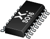
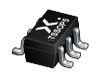
The 74LV4052-Q100 is a dual single-pole quad-throw analog switch suitable for use in 4:1 multiplexer/demultip
lexer applications. Each switch features four independent inputs/outputs (nY0, nY1, nY2 and nY3) and a common input/output (nZ). A digital enable input (E) and two digital select inputs (S0, S1) are common to both switches. When Eis HIGH, the switches are turned off. Digital inputs include clamp diodes. This enables the use of current limiting resistors to interface inputs to voltages in excess VCC.
This product has been qualified to the Automotive Electronics Council (AEC) standard Q100 (Grade 1) and is suitable for use in automotive applications.
Features and benefits
Automotive product qualification in accordance with AEC-Q100 (Grade 1)
Specified from -40 °C to +85 °C and from -40 °C to +125 °C
Wide supply voltage range from 1.0 to 6.0 V
CMOS low power dissipation
Latch-up performance exceeds 100 mA per JESD 78 Class II Level B
Optimized for low-voltage applications: 1.0 V to 6.0 V
Accepts TTL input levels between VCC = 2.7 V and VCC = 3.6 V
Low ON resistance:
145 Ω (typical) at VCC - VEE = 2.0 V
90 Ω (typical) at VCC - VEE = 3.0 V
60 Ω (typical) at VCC - VEE = 4.5 V
Logic level translation:
To enable 3 V logic to communicate with ± 3 V analog signals
Typical ‘break before make’ built in
Complies with JEDEC standards:
JESD8-7 (1.65 V to 1.95 V)
JESD8-5 (2.3 V to 2.7 V)
JESD8C (2.7 V to 3.6 V)
JESD36 (4.5 V to 5.5 V)
ESD protection:
HBM: ANSI/ESDA/JEDEC JS-001 class 2 exceeds 2000 V
CDM: ANSI/ESDA/JEDEC JS-002 class C3 exceeds 1000 V
The 74LV4052-Q100 is a dual single-pole quad-throw analog switch suitable for use in 4:1 multiplexer/demultiplexer applications. Each switch features four independent inputs/outputs (nY0, nY1, nY2 and nY3) and a common input/output (nZ). A digital enable input (E) and two digital select inputs (S0, S1) are common to both switches. When Eis HIGH, the switches are turned off. Digital inputs include clamp diodes. This enables the use of current limiting resistors to interface inputs to voltages in excess VCC.
This product has been qualified to the Automotive Electronics Council (AEC) standard Q100 (Grade 1) and is suitable for use in automotive applications.
Features and benefits
- Automotive product qualification in accordance with AEC-Q100 (Grade 1)
- Specified from -40 °C to +85 °C and from -40 °C to +125 °C
- Wide supply voltage range from 1.0 to 6.0 V
- CMOS low power dissipation
- Latch-up performance exceeds 100 mA per JESD 78 Class II Level B
- Optimized for low-voltage applications: 1.0 V to 6.0 V
- Accepts TTL input levels between VCC = 2.7 V and VCC = 3.6 V
- Low ON resistance:
- 145 Ω (typical) at VCC - VEE = 2.0 V
- 90 Ω (typical) at VCC - VEE = 3.0 V
- 60 Ω (typical) at VCC - VEE = 4.5 V
- Logic level translation:
- To enable 3 V logic to communicate with ± 3 V analog signals
- Typical ‘break before make’ built in
- Complies with JEDEC standards:
- JESD8-7 (1.65 V to 1.95 V)
- JESD8-5 (2.3 V to 2.7 V)
- JESD8C (2.7 V to 3.6 V)
- JESD36 (4.5 V to 5.5 V)
- ESD protection:
- HBM: ANSI/ESDA/JEDEC JS-001 class 2 exceeds 2000 V
- CDM: ANSI/ESDA/JEDEC JS-002 class C3 exceeds 1000 V