The 74LV138 decodes three binary weighted address inputs (A0, A1 and A2) to eight mutually exclusive outputs (Y0 to Y7). The 74LV138 features three enable inputs (Y1, Y2 and E3). Every output will be HIGH unless Y1 and Y2 are LOW and E3 is HIGH. This multiple enable function allows easy parallel expansion of the 74LV138 to a 1-of-32 (5 to 32 lines) decoder with just four 74LV138 ICs and one inverter. The 74LV138 can be used as an eight output demultiplexer by using one of the active LOW enable inputs as the data input and the remaining enable inputs as strobes. Inputs include clamp diodes. This enables the use of current limiting resistors to interface inputs to voltages in excess VCC.
Features and benefits
Wide supply voltage range from 1.0 to 5.5 V
Optimized for low voltage applications: 1.0 V to 3.6 V
CMOS low power dissipation
Direct interface with TTL levels
Typical output ground bounce < 0.8 V at VCC = 3.3 V and Tamb = 25 °C
Typical HIGH-level output voltage (VOH) undershoot: > 2 V at VCC = 3.3 V and Tamb = 25 °C
Demultiplexing capability
Multiple input enable for easy expansion
Ideal for memory chip select decoding
Active LOW mutually exclusive outputs
Latch-up performance exceeds 100 mA per JESD 78 Class II Level B
Complies with JEDEC standards
JESD8-7 (1.65 V to 1.95 V)
JESD8-5 (2.3 V to 2.7 V)
JESD8C (2.7 V to 3.6 V)
JESD36 (4.5 V to 5.5 V)
ESD protection:
HBM: ANSI/ESDA/JEDEC JS-001 class 2 exceeds 2000 V
CDM: ANSI/ESDA/JEDEC JS-002 class C3 exceeds 1000 V
Multiple package options
Specified from -40 °C to +85 °C and from -40 °C to +125 °C
The 74LV138 decodes three binary weighted address inputs (A0, A1 and A2) to eight mutually exclusive outputs (Y0 to Y7). The 74LV138 features three enable inputs (Y1, Y2 and E3). Every output will be HIGH unless Y1 and Y2 are LOW and E3 is HIGH. This multiple enable function allows easy parallel expansion of the 74LV138 to a 1-of-32 (5 to 32 lines) decoder with just four 74LV138 ICs and one inverter. The 74LV138 can be used as an eight output demultiplexer by using one of the active LOW enable inputs as the data input and the remaining enable inputs as strobes. Inputs include clamp diodes. This enables the use of current limiting resistors to interface inputs to voltages in excess VCC.
Features and benefits
- Wide supply voltage range from 1.0 to 5.5 V
- Optimized for low voltage applications: 1.0 V to 3.6 V
- CMOS low power dissipation
- Direct interface with TTL levels
- Typical output ground bounce < 0.8 V at VCC = 3.3 V and Tamb = 25 °C
- Typical HIGH-level output voltage (VOH) undershoot: > 2 V at VCC = 3.3 V and Tamb = 25 °C
- Demultiplexing capability
- Multiple input enable for easy expansion
- Ideal for memory chip select decoding
- Active LOW mutually exclusive outputs
- Latch-up performance exceeds 100 mA per JESD 78 Class II Level B
- Complies with JEDEC standards
- JESD8-7 (1.65 V to 1.95 V)
- JESD8-5 (2.3 V to 2.7 V)
- JESD8C (2.7 V to 3.6 V)
- JESD36 (4.5 V to 5.5 V)
- ESD protection:
- HBM: ANSI/ESDA/JEDEC JS-001 class 2 exceeds 2000 V
- CDM: ANSI/ESDA/JEDEC JS-002 class C3 exceeds 1000 V
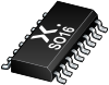
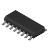
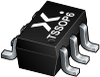
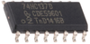
- Multiple package options
- Specified from -40 °C to +85 °C and from -40 °C to +125 °C