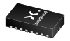
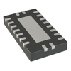
The 74HC574-Q100; 74HCT574-Q100 is an 8-bit positive-edge triggered D-type flip-flop with 3-state outputs. The device features a clock (CP) and output enable (OE) inputs. The flip-flops will store the state of their individual D-inputs that meet the set-up and hold time requirements on the LOW-to-HIGH clock (CP) transition. A HIGH on OEcauses the outputs to assume a high-impedance OFF-state. Operation of the OEinput does not affect the state of the flip-flops. Inputs include clamp diodes. This enables the use of current limiting resistors to interface inputs to voltages in excess of VCC.
This product has been qualified to the Automotive Electronics Council (AEC) standard Q100 (Grade 1) and is suitable for use in automotive applications.
Features and benefits
Automotive product qualification in accordance with AEC-Q100 (Grade 1)
Specified from -40 °C to +85 °C and from -40 °C to +125 °C
Wide supply voltage range from 2.0 V to 6.0 V
CMOS low power dissipation
High noise immunity
Latch-up performance exceeds 100 mA per JESD 78 Class II Level B
Complies with JEDEC standards:
JESD8C (2.7 V to 3.6 V)
JESD7A (2.0 V to 6.0 V)
Input levels:
For 74HC574-Q100: CMOS level
For 74HCT574-Q100: TTL level
3-state non-inverting outputs for bus oriented applications
8-bit positive, edge-triggered register
Common 3-state output enable input
ESD protection:
HBM: ANSI/ESDA/JEDEC JS-001 class 2 exceeds 2000 V
CDM: ANSI/ESDA/JEDEC JS-002 class C3 exceeds 1000 V
DHVQFN package with Side-Wettable Flanks enabling Automated Optical Inspection (AOI) of solder joints
The 74HC574-Q100; 74HCT574-Q100 is an 8-bit positive-edge triggered D-type flip-flop with 3-state outputs. The device features a clock (CP) and output enable (OE) inputs. The flip-flops will store the state of their individual D-inputs that meet the set-up and hold time requirements on the LOW-to-HIGH clock (CP) transition. A HIGH on OEcauses the outputs to assume a high-impedance OFF-state. Operation of the OEinput does not affect the state of the flip-flops. Inputs include clamp diodes. This enables the use of current limiting resistors to interface inputs to voltages in excess of VCC.
This product has been qualified to the Automotive Electronics Council (AEC) standard Q100 (Grade 1) and is suitable for use in automotive applications.
Features and benefits
- Automotive product qualification in accordance with AEC-Q100 (Grade 1)
- Specified from -40 °C to +85 °C and from -40 °C to +125 °C
- Wide supply voltage range from 2.0 V to 6.0 V
- CMOS low power dissipation
- High noise immunity
- Latch-up performance exceeds 100 mA per JESD 78 Class II Level B
- Complies with JEDEC standards:
- JESD8C (2.7 V to 3.6 V)
- JESD7A (2.0 V to 6.0 V)
- Input levels:
- For 74HC574-Q100: CMOS level
- For 74HCT574-Q100: TTL level
- 3-state non-inverting outputs for bus oriented applications
- 8-bit positive, edge-triggered register
- Common 3-state output enable input
- ESD protection:
- HBM: ANSI/ESDA/JEDEC JS-001 class 2 exceeds 2000 V
- CDM: ANSI/ESDA/JEDEC JS-002 class C3 exceeds 1000 V
- DHVQFN package with Side-Wettable Flanks enabling Automated Optical Inspection (AOI) of solder joints