
The 74CBTLV3253 provides a dual 1-of-4 high-speed multiplexer/demultip
To ensure the high-impedance OFF-state during power-up or power-down, nOE should be tied to the VCC through a pull-up resistor. The minimum value of the resistor is determined by the current-sinking capability of the driver.
Schmitt trigger action at control input makes the circuit tolerant to slower input rise and fall times across the entire VCC range from 2.3 V to 3.6 V.
This device is fully specified for partial power-down applications using IOFF. The IOFF circuitry disables the output, preventing the damaging backflow current through the device when it is powered down.
Features and benefits
Multiplexer/Demultip
Multiplexer/Demultip
Multiplexer/Demultip
Multiplexer/Demultip
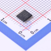
2.3V~3.6V TSSOP-16 Signal Switches / Encoders & Decoders / Multiplexers ROHS
IC MUX/DEMUX 2 X 4:1 16TSSOP
| Nexperia B.V. | DigiKey | ERSAELECTRONICS PTE. LTD. | LCSC Electronics Technology (HK) Limited | Lingto Electronic Limited | |
|---|---|---|---|---|---|
| Product Category | IC Analog Multiplexers | IC Analog Multiplexers | IC Analog Multiplexers | IC Analog Multiplexers | IC Analog Multiplexers |
| Product Number | 74CBTLV3253PW,118 | 1727-4407-1-ND | 743-74CBTLV3253PW,118 | 74CBTLV3253PW,118 | 74CBTLV3253PW,118 |
| Product Name | Dual 1-of-4 multiplexer/demultiplexer | Signal Switches, Multiplexers, Decoders | TSSOP Analog Switch and Multiplexer IC | Logic ICs >> Signal Switches / Encoders & Decoders / Multiplexers | Logic - Signal Switches, Multiplexers, Decoders |
| Features | On-Chip ESD Protection | ||||
| Standards and Certifications | RoHS | RoHS | |||
| Supply Voltage (VS) | 2.3 to 3.6 volts | 2.3 to 3.6 volts | |||
| Ron | 7 ohms |