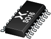
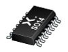
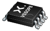
The 74AHC139-Q100; 74AHCT139-Q100 decodes two binary weighted address inputs (nA0, nA1) to four mutually exclusive outputs (nY0 to nY3). Each decoder features an enable input (nE). When nEis HIGH all outputs are forced HIGH. The enable input can be used as the data input for a 1-to-4 demultiplexer application. Inputs are overvoltage tolerant. This feature allows the use of these devices as translators in mixed voltage environments.
This product has been qualified to the Automotive Electronics Council (AEC) standard Q100 (Grade 1) and is suitable for use in automotive applications.
Features and benefits
Automotive product qualification in accordance with AEC-Q100 (Grade 1)
Specified from -40 °C to +85 °C and from -40 °C to +125 °C
Wide supply voltage range from 2.0 to 5.5 V
Balanced propagation delays
High noise immunity
CMOS low power dissipation
All inputs have Schmitt-trigger actions
Overvoltage tolerant inputs to 5.5 V
Input levels:
For 74AHC139-Q100: CMOS level
For 74AHCT139-Q100: TTL level
Latch-up performance exceeds 100 mA per JESD 78 Class II Level A
ESD protection:
HBM: ANSI/ESDA/JEDEC JS-001 class 2 exceeds 2000 V
CDM: ANSI/ESDA/JEDEC JS-002 class C3 exceeds 1000 V
The 74AHC139-Q100; 74AHCT139-Q100 decodes two binary weighted address inputs (nA0, nA1) to four mutually exclusive outputs (nY0 to nY3). Each decoder features an enable input (nE). When nEis HIGH all outputs are forced HIGH. The enable input can be used as the data input for a 1-to-4 demultiplexer application. Inputs are overvoltage tolerant. This feature allows the use of these devices as translators in mixed voltage environments.
This product has been qualified to the Automotive Electronics Council (AEC) standard Q100 (Grade 1) and is suitable for use in automotive applications.
Features and benefits
- Automotive product qualification in accordance with AEC-Q100 (Grade 1)
- Specified from -40 °C to +85 °C and from -40 °C to +125 °C
- Wide supply voltage range from 2.0 to 5.5 V
- Balanced propagation delays
- High noise immunity
- CMOS low power dissipation
- All inputs have Schmitt-trigger actions
- Overvoltage tolerant inputs to 5.5 V
- Input levels:
- For 74AHC139-Q100: CMOS level
- For 74AHCT139-Q100: TTL level
- Latch-up performance exceeds 100 mA per JESD 78 Class II Level A
- ESD protection:
- HBM: ANSI/ESDA/JEDEC JS-001 class 2 exceeds 2000 V
- CDM: ANSI/ESDA/JEDEC JS-002 class C3 exceeds 1000 V