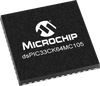
Microchip’s dsPIC33CK64MC10X family of Digital Signal Controllers (DSCs) features a single 100 MIPS dsPIC® DSC core with integrated DSP and enhanced on-chip peripherals. These DSCs enable the design of automotive, motor control, high-performance and robust applications. In the motor control segment, this family is well suited for cost competitive automotive, consumer and industrial applications. The dsPIC33CK64MC105 family of DSCs are ideal for the control of BLDC, PMSM, ACIM, SR and stepper motors. The high level of peripheral integration on the dsPIC33CK64MC105 enable applications to implement power factor correction (PFC) and Motor Control using a single DSC.
Loaded with intelligent analog peripherals, such as high-performance ADCs and DACs, high-speed comparators, and op amps, dsPIC33CK64MC10X family of DSCs provide simple-to-use smart sensor interfaces for various electronic sensing applications. The rich feature set and 150°C high-temperature rating available on this DSC family make it a very good fit for automotive sensors and industrial automation.
The dsPIC33CK product family has many features that help simplify functional safety certifications for ASIL-B and ASIL-C focused applications including: • Functional Safety Manual, FMEDA and Diagnostic Software available under NDA upon request to your local sales office • Learn more about 16-bit Functional Safety capabilities including hardware, software, and supporting collateral
Additional Features
Operating Conditions
3.0 V to 3.6 V
-40ºC to +125ºC, DC to 100 MIPS
-40ºC to +150ºC, DC to 70 MIPS
dsPIC33CK DSC Core
Up to 64 KBytes of Program Flash with ECC and Fault Injection testing feature
Up to 8 KBytes of Data SRAM with Memory Built in Self-Test (MBIST)
Modified Harvard architecture with 16-bit data and 24-bit instructions
Code efficient (C and Assembly) CPU architecture designed for real-time applications
Sixteen 16-bit working registers
Four sets of interrupt context saving registers, including ACC and CPU status for fast interrupt handling
Single-cycle, mixed-sign 32-bit multiplication
Fast 6-cycle hardware 32/16 and 16/16 DIV
Dual 40-bit fixed point Accumulators (ACC) for DSP operations
Single-cycle MAC/MPY with dual data fetch and result write-back
Zero overhead looping support
High-Speed PWM Module
Four independent PWM pairs (Eight total outputs) with up to 2 ns resolution
Dead-time insertion for rising and falling edges and dead-time compensation support
Clock chopping for high-frequency operation
Fault and current limit inputs
Flexible trigger configuration for ADC triggering
Advanced Analog Features
12-bit 3.5 MSPS ADC Module
Up to 15 ADC input channels (depending on package)
Four digital comparators for reducing CPU overhead
Four oversampling filers up to 256x for increased resolution (up to 16-bits)
One analog comparator (15ns) with dedicated 12-bit DAC with hardware slope compensation and DAC buffer output
Up to three op amps with internal connection to ADC Module
Timer/Counters/Outpu
t Compare/Input Capture
One Dedicated 16-Bit Timer/Counter
Four SCCP - Flexible configuration as four PWM outputs (down to 4ns resolution), input capture, output compare, eight 16-bit timer/counters or up to four 32-bit timer/counters
Peripheral Trigger Generator (PTG) for scheduling complex sequences or alternate configuration as two 16-bit timer
Quadrature Encoder Interface (QEI) Modules for optical encoder support or alternate configuration as a 32-bit timer
Communication Interfaces
Three UARTs (15 Mbps) with automated protocol handling for LIN/J2602 and DMX
Two 4-wire SPI/I2S up to 40 MHz with dedicated pins
One I2C Modules (up to 1 Mbps) with SMBus support
One Single-Edge Nibble Transmission (SENT) Modules for sensor interfacing
Four DMA channels supporting data transfers
Special Features
Four Configurable Logic Cell (CLC) Modules with user defined logic gate circuits
Programmable Pin Select (PPS) for peripheral pin function mapping
On-chip temperature sensor with direct ADC Module connection
256 Bytes of One-Time-Programmabl
e (OTP) Memory and 120-bit Unique Device Identifier (UDID)
Clock and Power Management
On-chip 8 MHz Fast RC (FRC)
Programmable PLLs with external oscillator clock sources and Reference Clock Output (REFO)
Fail-Safe Clock Monitor (FSCM) with 8 MHz Back-up Fast RC (BFRC) oscillator
Low-Power management modes - Sleep, Idle and Doze
Integrated Power-on Reset (POR) and Brown-Out Reset (BOR)
Debugger Development Support
In-Circuit and in application programming and debug support (ICSP)
On-chip debug with 3 complex and 5 simple breakpoints
IEEE 1149.2 (JTAG) boundary scan support
Safety Features
Dead-Man Timer (DMT) safety feature clocked by instruction fetches
Windowed Watch Dog Timer (WWDT)
CodeGuard™ security for program FLASH
FLASH with ECC and Fault Injection testing feature
Flash OTP by ICSP™ write inhibit
Memory Built in Self-Test (MBIST)
Clock Monitor with multiple redundant clock sources
Programmable Cyclic Redundancy Check (CRC)
Hardware traps
SFR locks
Shadow working registers
PWM Fault Management
cap-less on-chip LDO
I/O Port read-back
Class B Safety Library, IEC 60730
Functional Safety support (ISO26262)
Ideal for ASIL-B & ASIL-C focused applications
FMEDA, Diagnostic Software and Functional Safety manual available under NDA upon request to your sales office
Microchip’s dsPIC33CK64MC10X family of Digital Signal Controllers (DSCs) features a single 100 MIPS dsPIC® DSC core with integrated DSP and enhanced on-chip peripherals. These DSCs enable the design of automotive, motor control, high-performance and robust applications.
In the motor control segment, this family is well suited for cost competitive automotive, consumer and industrial applications. The dsPIC33CK64MC105 family of DSCs are ideal for the control of BLDC, PMSM, ACIM, SR and stepper motors. The high level of peripheral integration on the dsPIC33CK64MC105 enable applications to implement power factor correction (PFC) and Motor Control using a single DSC.
Loaded with intelligent analog peripherals, such as high-performance ADCs and DACs, high-speed comparators, and op amps, dsPIC33CK64MC10X family of DSCs provide simple-to-use smart sensor interfaces for various electronic sensing applications. The rich feature set and 150°C high-temperature rating available on this DSC family make it a very good fit for automotive sensors and industrial automation.
The dsPIC33CK product family has many features that help simplify functional safety certifications for ASIL-B and ASIL-C focused applications including:
• Functional Safety Manual, FMEDA and Diagnostic Software available under NDA upon request to your local sales office
• Learn more about 16-bit Functional Safety capabilities including hardware, software, and supporting collateral
Additional Features
- Operating Conditions
- 3.0 V to 3.6 V
- -40ºC to +125ºC, DC to 100 MIPS
- -40ºC to +150ºC, DC to 70 MIPS
- dsPIC33CK DSC Core
- Up to 64 KBytes of Program Flash with ECC and Fault Injection testing feature
- Up to 8 KBytes of Data SRAM with Memory Built in Self-Test (MBIST)
- Modified Harvard architecture with 16-bit data and 24-bit instructions
- Code efficient (C and Assembly) CPU architecture designed for real-time applications
- Sixteen 16-bit working registers
- Four sets of interrupt context saving registers, including ACC and CPU status for fast interrupt handling
- Single-cycle, mixed-sign 32-bit multiplication
- Fast 6-cycle hardware 32/16 and 16/16 DIV
- Dual 40-bit fixed point Accumulators (ACC) for DSP operations
- Single-cycle MAC/MPY with dual data fetch and result write-back
- Zero overhead looping support
- High-Speed PWM Module
- Four independent PWM pairs (Eight total outputs) with up to 2 ns resolution
- Dead-time insertion for rising and falling edges and dead-time compensation support
- Clock chopping for high-frequency operation
- Fault and current limit inputs
- Flexible trigger configuration for ADC triggering
- Advanced Analog Features
- 12-bit 3.5 MSPS ADC Module
- Up to 15 ADC input channels (depending on package)
- Four digital comparators for reducing CPU overhead
- Four oversampling filers up to 256x for increased resolution (up to 16-bits)
- One analog comparator (15ns) with dedicated 12-bit DAC with hardware slope compensation and DAC buffer output
- Up to three op amps with internal connection to ADC Module
- Timer/Counters/Output Compare/Input Capture
- One Dedicated 16-Bit Timer/Counter
- Four SCCP - Flexible configuration as four PWM outputs (down to 4ns resolution), input capture, output compare, eight 16-bit timer/counters or up to four 32-bit timer/counters
- Peripheral Trigger Generator (PTG) for scheduling complex sequences or alternate configuration as two 16-bit timer
- Quadrature Encoder Interface (QEI) Modules for optical encoder support or alternate configuration as a 32-bit timer
- Communication Interfaces
- Three UARTs (15 Mbps) with automated protocol handling for LIN/J2602 and DMX
- Two 4-wire SPI/I2S up to 40 MHz with dedicated pins
- One I2C Modules (up to 1 Mbps) with SMBus support
- One Single-Edge Nibble Transmission (SENT) Modules for sensor interfacing
- Four DMA channels supporting data transfers
- Special Features
- Four Configurable Logic Cell (CLC) Modules with user defined logic gate circuits
- Programmable Pin Select (PPS) for peripheral pin function mapping
- On-chip temperature sensor with direct ADC Module connection
- 256 Bytes of One-Time-Programmable (OTP) Memory and 120-bit Unique Device Identifier (UDID)
- Clock and Power Management
- On-chip 8 MHz Fast RC (FRC)
- Programmable PLLs with external oscillator clock sources and Reference Clock Output (REFO)
- Fail-Safe Clock Monitor (FSCM) with 8 MHz Back-up Fast RC (BFRC) oscillator
- Low-Power management modes - Sleep, Idle and Doze
- Integrated Power-on Reset (POR) and Brown-Out Reset (BOR)
- Debugger Development Support
- In-Circuit and in application programming and debug support (ICSP)
- On-chip debug with 3 complex and 5 simple breakpoints
- IEEE 1149.2 (JTAG) boundary scan support
- Safety Features
- Dead-Man Timer (DMT) safety feature clocked by instruction fetches
- Windowed Watch Dog Timer (WWDT)
- CodeGuard™ security for program FLASH
- FLASH with ECC and Fault Injection testing feature
- Flash OTP by ICSP™ write inhibit
- Memory Built in Self-Test (MBIST)
- Clock Monitor with multiple redundant clock sources
- Programmable Cyclic Redundancy Check (CRC)
- Hardware traps
- SFR locks
- Shadow working registers
- PWM Fault Management
- cap-less on-chip LDO
- I/O Port read-back
- Class B Safety Library, IEC 60730
- Functional Safety support (ISO26262)
- Ideal for ASIL-B & ASIL-C focused applications
- FMEDA, Diagnostic Software and Functional Safety manual available under NDA upon request to your sales office