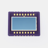
Hamamatsu Photonics Europe Si photodiodes S7510

Description
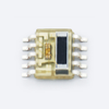
The S7510 is a Si PIN photodiode sealed in chip carrier packages suitable for surface mount using automated solder reflow techniques. This photodiode has a large photosensitive area, making it suitable for spatial light transmission where a wide field-of-view angle is required. Other applications include POS scanners, power meters and analytical instruments. Features - Photosensitive area: 6 × 11 mm - Ceramic chip carrier package for surface mount - Suitable for solder reflow - High sensitivity - Packing Tray: S7510 Reel: S7510-10
Request a Quote Datasheet
Description
The S7510 is a Si PIN photodiode sealed in chip carrier packages suitable for surface mount using automated solder reflow techniques. This photodiode has a large photosensitive area, making it suitable for spatial light transmission where a wide field-of-view angle is required. Other applications include POS scanners, power meters and analytical instruments. Features - Photosensitive area: 6 × 11 mm - Ceramic chip carrier package for surface mount - Suitable for solder reflow - High sensitivity - Packing Tray: S7510 Reel: S7510-10
Request a Quote Datasheet

Suppliers

Company
Product
Description
Supplier Links
Si photodiodes - S7510 - Hamamatsu Photonics Europe
Herrsching am Ammersee, Germany
Si photodiodes
S7510
Si photodiodes S7510
The S7510 is a Si PIN photodiode sealed in chip carrier packages suitable for surface mount using automated solder reflow techniques. This photodiode has a large photosensitive area, making it suitable for spatial light transmission where a wide field-of-view angle is required. Other applications include POS scanners, power meters and analytical instruments. Features - Photosensitive area: 6 × 11 mm - Ceramic chip carrier package for surface mount - Suitable for solder reflow - High sensitivity - Packing Tray: S7510 Reel: S7510-10

The S7510 is a Si PIN photodiode sealed in chip carrier packages suitable for surface mount using automated solder reflow techniques. This photodiode has a large photosensitive area, making it suitable for spatial light transmission where a wide field-of-view angle is required. Other applications include POS scanners, power meters and analytical instruments.

Features
- Photosensitive area: 6 × 11 mm
- Ceramic chip carrier package for surface mount
- Suitable for solder reflow
- High sensitivity
- Packing
Tray: S7510
Reel: S7510-10

Supplier's Site Datasheet

Technical Specifications

  Hamamatsu Photonics Europe
Product Category Photodiodes
Product Number S7510
Product Name Si photodiodes
Photodiode Type PIN Photodiode
Spectral Response Range 320 to 1100 nm (3200 to 11000 Å)
Peak Sensitivity Wavelength 960 nm (9600 Å)
Photodiode Material Silicon
Unlock Full Specs
to access all available technical data

Similar Products

Si photodiode arrays with amplifier - S11865-64 - Hamamatsu Photonics Europe
Specs
Photodiode Spectral Response X-ray
Spectral Response Range 200 to 1000 nm (2000 to 10000 Å)
Peak Sensitivity Wavelength 720 nm (7200 Å)
View Details
Si photodiodes - S16839-01MS - Hamamatsu Photonics Europe
Hamamatsu Photonics Europe
Specs
Photodiode Spectral Response Visible
Spectral Response Range 480 to 660 nm (4800 to 6600 Å)
Peak Sensitivity Wavelength 550 nm (5500 Å)
View Details
Si photodiodes - S14536-500 - Hamamatsu Photonics Europe
Hamamatsu Photonics Europe
Specs
Photodiode Material Silicon
Active Area Diameter or Length 48 mm (1.89 inch)
Active Area Height 48 mm (1.89 inch)
View Details
Si photodiode arrays - S12858-021 - Hamamatsu Photonics Europe
Hamamatsu Photonics Europe
Specs
Photodiode Spectral Response X-ray
Spectral Response Range 340 to 1100 nm (3400 to 11000 Å)
Peak Sensitivity Wavelength 920 nm (9200 Å)
View Details