FX PCB Co., Ltd. 6 Layer PCB

Description
Description 6-Layer PCB Vs 4-Layer PCB? A 6-layer PCB is a printed circuit board made up of six layers of material, created using chemical etching. Compared to double-sided and 4-layer PCBs, 6-layer PCBs offer more circuit layers, higher wiring density, and better resistance to interference. Additionally, advanced techniques like blind vias and buried vias can be used to further enhance Manufacturing Process of 6-Layer PCBs The manufacturing process of a 6-layer PCB includes the following steps: material selection, circuit design, inner and outer layer production, pattern transfer, chemical etching, electroplating, drilling, circuit pattern deposition, copper lamination, CNC, and testing. Inner and outer layer production, chemical etching, and electroplating are critical steps that directly affect the quality and performance of the PCB. 6-layer PCBs are widely used high-performance printed circuit boards in modern electronics, offering advantages like multilayer routing, high density, and high-speed signal transmission. During the design process, following specific layer design rules is crucial, such as ensuring symmetrical inner layer layouts, isolating signal layers from ground layers, avoiding ground layers between adjacent signal layers, and minimizing the number of vias. By carefully controlling each step of the manufacturing process, high-quality and high-performance 6-layer PCBs can be produced, providing a reliable foundation for the development of modern electronic products. Capability of 6-Layer PCB Layers: 6 Material: FR4 Thickness: 0.6mm – 10mm Copper Weight: 1/2oz – 10oz per layer Surface Finish: HASL, ENIG, OSP, or others Min. Line Width/Spacing: 0.07mm/0.07mm Min. Hole Size: 0.15mm Impedance Control: YES Blinded and Buried Holes: YES Why Choose FX PCB 6-Layer PCBs? Advanced Manufacturing Process: Leveraging cutting-edge technology to deliver flawless multilayer boards. Fast Turnaround Times: Quick prototyping and production to keep your project on schedule. Strict Quality Control: Every PCB will be tested before shipping to ensure it meets or exceeds industry standards. Eco-Friendly Practices: All PCBs are Rohs and Reach meet How to Order Getting started is easy: Submit your design files (Gerber). Specify your material, thickness, finish, and any special requirements. Receive a free quote within 24 hours. Approve and place your order. Get your PCBs delivered fast! Frequently Asked Questions Q: What kind of file you can use to produce the PCB? Gerber file, eagle file, PCB file Q: What kind of payment can you make? TT, Paypal, Payoneer, WeChat Pay, Alipay Q: What is your lead time? A: Standard production takes 5-10 business days. Expedited services are available upon request. Get Started Today Don’t settle for less when your projects demand the best. Contact FX PCB now for a free consultation or to request a quote. Let’s bring your designs to life with our high-quality 6-layer PCBs.
Request a Quote
Description
Description 6-Layer PCB Vs 4-Layer PCB? A 6-layer PCB is a printed circuit board made up of six layers of material, created using chemical etching. Compared to double-sided and 4-layer PCBs, 6-layer PCBs offer more circuit layers, higher wiring density, and better resistance to interference. Additionally, advanced techniques like blind vias and buried vias can be used to further enhance Manufacturing Process of 6-Layer PCBs The manufacturing process of a 6-layer PCB includes the following steps: material selection, circuit design, inner and outer layer production, pattern transfer, chemical etching, electroplating, drilling, circuit pattern deposition, copper lamination, CNC, and testing. Inner and outer layer production, chemical etching, and electroplating are critical steps that directly affect the quality and performance of the PCB. 6-layer PCBs are widely used high-performance printed circuit boards in modern electronics, offering advantages like multilayer routing, high density, and high-speed signal transmission. During the design process, following specific layer design rules is crucial, such as ensuring symmetrical inner layer layouts, isolating signal layers from ground layers, avoiding ground layers between adjacent signal layers, and minimizing the number of vias. By carefully controlling each step of the manufacturing process, high-quality and high-performance 6-layer PCBs can be produced, providing a reliable foundation for the development of modern electronic products. Capability of 6-Layer PCB Layers: 6 Material: FR4 Thickness: 0.6mm – 10mm Copper Weight: 1/2oz – 10oz per layer Surface Finish: HASL, ENIG, OSP, or others Min. Line Width/Spacing: 0.07mm/0.07mm Min. Hole Size: 0.15mm Impedance Control: YES Blinded and Buried Holes: YES Why Choose FX PCB 6-Layer PCBs? Advanced Manufacturing Process: Leveraging cutting-edge technology to deliver flawless multilayer boards. Fast Turnaround Times: Quick prototyping and production to keep your project on schedule. Strict Quality Control: Every PCB will be tested before shipping to ensure it meets or exceeds industry standards. Eco-Friendly Practices: All PCBs are Rohs and Reach meet How to Order Getting started is easy: Submit your design files (Gerber). Specify your material, thickness, finish, and any special requirements. Receive a free quote within 24 hours. Approve and place your order. Get your PCBs delivered fast! Frequently Asked Questions Q: What kind of file you can use to produce the PCB? Gerber file, eagle file, PCB file Q: What kind of payment can you make? TT, Paypal, Payoneer, WeChat Pay, Alipay Q: What is your lead time? A: Standard production takes 5-10 business days. Expedited services are available upon request. Get Started Today Don’t settle for less when your projects demand the best. Contact FX PCB now for a free consultation or to request a quote. Let’s bring your designs to life with our high-quality 6-layer PCBs.
Request a Quote

Suppliers

Company
Product
Description
Supplier Links
6 Layer PCB -  - FX PCB Co., Ltd.
Shenzhen, Guangdong, China
6 Layer PCB
6 Layer PCB
Description 6-Layer PCB Vs 4-Layer PCB? A 6-layer PCB is a printed circuit board made up of six layers of material, created using chemical etching. Compared to double-sided and 4-layer PCBs, 6-layer PCBs offer more circuit layers, higher wiring density, and better resistance to interference. Additionally, advanced techniques like blind vias and buried vias can be used to further enhance Manufacturing Process of 6-Layer PCBs The manufacturing process of a 6-layer PCB includes the following steps: material selection, circuit design, inner and outer layer production, pattern transfer, chemical etching, electroplating, drilling, circuit pattern deposition, copper lamination, CNC, and testing. Inner and outer layer production, chemical etching, and electroplating are critical steps that directly affect the quality and performance of the PCB. 6-layer PCBs are widely used high-performance printed circuit boards in modern electronics, offering advantages like multilayer routing, high density, and high-speed signal transmission. During the design process, following specific layer design rules is crucial, such as ensuring symmetrical inner layer layouts, isolating signal layers from ground layers, avoiding ground layers between adjacent signal layers, and minimizing the number of vias. By carefully controlling each step of the manufacturing process, high-quality and high-performance 6-layer PCBs can be produced, providing a reliable foundation for the development of modern electronic products. Capability of 6-Layer PCB Layers: 6 Material: FR4 Thickness: 0.6mm – 10mm Copper Weight: 1/2oz – 10oz per layer Surface Finish: HASL, ENIG, OSP, or others Min. Line Width/Spacing: 0.07mm/0.07mm Min. Hole Size: 0.15mm Impedance Control: YES Blinded and Buried Holes: YES Why Choose FX PCB 6-Layer PCBs? Advanced Manufacturing Process: Leveraging cutting-edge technology to deliver flawless multilayer boards. Fast Turnaround Times: Quick prototyping and production to keep your project on schedule. Strict Quality Control: Every PCB will be tested before shipping to ensure it meets or exceeds industry standards. Eco-Friendly Practices: All PCBs are Rohs and Reach meet How to Order Getting started is easy: Submit your design files (Gerber). Specify your material, thickness, finish, and any special requirements. Receive a free quote within 24 hours. Approve and place your order. Get your PCBs delivered fast! Frequently Asked Questions Q: What kind of file you can use to produce the PCB? Gerber file, eagle file, PCB file Q: What kind of payment can you make? TT, Paypal, Payoneer, WeChat Pay, Alipay Q: What is your lead time? A: Standard production takes 5-10 business days. Expedited services are available upon request. Get Started Today Don’t settle for less when your projects demand the best. Contact FX PCB now for a free consultation or to request a quote. Let’s bring your designs to life with our high-quality 6-layer PCBs.

Description

6-Layer PCB Vs 4-Layer PCB?

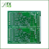
A 6-layer PCB is a printed circuit board made up of six layers of material, created using chemical etching. Compared to double-sided and 4-layer PCBs, 6-layer PCBs offer more circuit layers, higher wiring density, and better resistance to interference. Additionally, advanced techniques like blind vias and buried vias can be used to further enhance

Manufacturing Process of 6-Layer PCBs

The manufacturing process of a 6-layer PCB includes the following steps:

material selection, circuit design, inner and outer layer production, pattern transfer, chemical etching, electroplating, drilling, circuit pattern deposition, copper lamination, CNC, and testing. Inner and outer layer production, chemical etching, and electroplating are critical steps that directly affect the quality and performance of the PCB.

6-layer PCBs are widely used high-performance printed circuit boards in modern electronics, offering advantages like multilayer routing, high density, and high-speed signal transmission. During the design process, following specific layer design rules is crucial, such as ensuring symmetrical inner layer layouts, isolating signal layers from ground layers, avoiding ground layers between adjacent signal layers, and minimizing the number of vias. By carefully controlling each step of the manufacturing process, high-quality and high-performance 6-layer PCBs can be produced, providing a reliable foundation for the development of modern electronic products.

Capability of 6-Layer PCB

Layers: 6

Material: FR4

Thickness: 0.6mm – 10mm

Copper Weight: 1/2oz – 10oz per layer

Surface Finish: HASL, ENIG, OSP, or others

Min. Line Width/Spacing: 0.07mm/0.07mm

Min. Hole Size: 0.15mm

Impedance Control: YES

Blinded and Buried Holes: YES

Why Choose FX PCB 6-Layer PCBs?

  1. Advanced Manufacturing Process: Leveraging cutting-edge technology to deliver flawless multilayer boards.
  2. Fast Turnaround Times: Quick prototyping and production to keep your project on schedule.
  3. Strict Quality Control: Every PCB will be tested before shipping to ensure it meets or exceeds industry standards.
  4. Eco-Friendly Practices: All PCBs are Rohs and Reach meet

How to Order

Getting started is easy:

  1. Submit your design files (Gerber).
  2. Specify your material, thickness, finish, and any special requirements.
  3. Receive a free quote within 24 hours.
  4. Approve and place your order.
  5. Get your PCBs delivered fast!

Frequently Asked Questions

Q: What kind of file you can use to produce the PCB?

Gerber file, eagle file, PCB file

Q: What kind of payment can you make?

TT, Paypal, Payoneer, WeChat Pay, Alipay

Q: What is your lead time?

A: Standard production takes 5-10 business days. Expedited services are available upon request.

Get Started Today

Don’t settle for less when your projects demand the best. Contact FX PCB now for a free consultation or to request a quote. Let’s bring your designs to life with our high-quality 6-layer PCBs.
Supplier's Site

Technical Specifications

  FX PCB Co., Ltd.
Product Category Printed Circuit Substrate Materials (PCB / PWB)
Product Name 6 Layer PCB
Unlock Full Specs
to access all available technical data

Similar Products

Rigid-Flex PCB 6 Layer -  - FX PCB Co., Ltd.
Specs
Type Film / Flexible; Rigid
Materials Fr4+PI
Thickness 0.0394 inches (1 mm)
View Details
Glass PCB 3 -  - FX PCB Co., Ltd.
FX PCB Co., Ltd.
Specs
Materials Tempered low iron glass; Float glass; Sapphire crystal glass; Quartz glass
Thickness 0.0197 to 0.1969 inches (0.5000 to 5 mm)
View Details