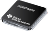
The XCalibur5090 is a high-performance, reconfigurable, conduction-cooled 6U LRM module based on the AMD (formerly Xilinx) Virtex-7 family of FPGAs. With a pair of Virtex-7 FPGA, high-speed serial interfaces, DAC and ADC channels, external memory, and flexible, high-density I/O, the XCalibur5090 is ideal for customizable, high-bandwidth, signal-processing applications.
The XCalibur5090 utilizes four AD9739 and two ADC12D1600RF to provide four channels of high-frequency 14-bit Digital Analog Conversion (DAC) at 2500 Mbps and four channels of 12-bit Analog Digital Conversion (ADC) at 1600 Mbps for high-performance Digital Signal Processing (DSP), which can also be used as two channels at 3200 Mbps.
The XCalibur5090 provides a high-performance, feature-rich solution capable of interfacing to and processing streaming data from a wide variety of sensors. The X-ES FPGA Development Kit (FDK) is provided to support the requirements of high-performance, real-time, embedded streaming data applications and simplify FPGA development. It includes IP blocks, example FPGA designs, and software to control and communicate with FPGAs.
Features
Two AMD (formerly Xilinx) Virtex-7 XC7VX690T FPGAs
Up to 1 GB of DDR3 SDRAM per FPGA in two channels
Non-volatile FPGA configuration flash
128 MB of user NOR flash per FPGA
Conduction-cooled 6U LRM form factor
Four 14-bit 2500 MSPS AD9739 DAC
Two dual-channel 12-bit 3200 MSPS ADC12D1600RF ADC
234 single-ended FPGA interconnects
Eight high-speed serial FPGA interconnects
28 FPGA GPO to the backplane
51 FPGA GPI from the backplane
17 FPGA GPIO to the backplane
FPGA Development Kit (FDK)
Technical Specs
FPGA
Dual AMD (formerly Xilinx) Virtex-7 for high-performance logic and DSP applications
Up to 1 GB of DDR3 SDRAM per FPGA in two channels
128 MB of user NOR flash per FPGA
x8 GTX interconnect between FPGAs
234 single-ended interconnect between FPGA
Supported FPGAs
Virtex-7 XC7VX690T
Support for commercial and industrial temperature as well as -1, -2, -3 speed grades
Development Support
X-ES FPGA Development Kit (FDK)
LRM Backplane I/O
x1 GTX
28 3.3 V CMOS from FPGA
51 3.3 V CMOS to FPGA
17 3.3 V CMOS GPIO to FPGA
x1 RF REFCLK input
x4 RF ADC inputs
x4 RF DAC outputs
Additional Features
Debug access connector
Debug LEDs
JTAG
x10 1.8 V GPIO to FPGA
Physical Characteristics
6U LRM conduction-cooled form factor
Dimensions: 233 mm x 164 mm
0.8 in. pitch without solder-side cover
0.85 in. and 1.0 in. pitch with solder-side cover
Environmental Requirements
Contact factory for appropriate board configuration based on environmental requirements.
Supported ruggedization levels (see the X-ES Ruggedization Chart): 1, 3, 5
Conformal coating available as an ordering option
Power Requirements
Power will vary based on configuration and usage. Please consult factory.
The XCalibur5090 is a high-performance, reconfigurable, conduction-cooled 6U LRM module based on the AMD (formerly Xilinx) Virtex-7 family of FPGAs. With a pair of Virtex-7 FPGA, high-speed serial interfaces, DAC and ADC channels, external memory, and flexible, high-density I/O, the XCalibur5090 is ideal for customizable, high-bandwidth, signal-processing applications.
The XCalibur5090 utilizes four AD9739 and two ADC12D1600RF to provide four channels of high-frequency 14-bit Digital Analog Conversion (DAC) at 2500 Mbps and four channels of 12-bit Analog Digital Conversion (ADC) at 1600 Mbps for high-performance Digital Signal Processing (DSP), which can also be used as two channels at 3200 Mbps.
The XCalibur5090 provides a high-performance, feature-rich solution capable of interfacing to and processing streaming data from a wide variety of sensors. The X-ES FPGA Development Kit (FDK) is provided to support the requirements of high-performance, real-time, embedded streaming data applications and simplify FPGA development. It includes IP blocks, example FPGA designs, and software to control and communicate with FPGAs.
Features
- Two AMD (formerly Xilinx) Virtex-7 XC7VX690T FPGAs
- Up to 1 GB of DDR3 SDRAM per FPGA in two channels
- Non-volatile FPGA configuration flash
- 128 MB of user NOR flash per FPGA
- Conduction-cooled 6U LRM form factor
- Four 14-bit 2500 MSPS AD9739 DAC
- Two dual-channel 12-bit 3200 MSPS ADC12D1600RF ADC
- 234 single-ended FPGA interconnects
- Eight high-speed serial FPGA interconnects
- 28 FPGA GPO to the backplane
- 51 FPGA GPI from the backplane
- 17 FPGA GPIO to the backplane
- FPGA Development Kit (FDK)
Technical Specs
FPGA
- Dual AMD (formerly Xilinx) Virtex-7 for high-performance logic and DSP applications
- Up to 1 GB of DDR3 SDRAM per FPGA in two channels
- 128 MB of user NOR flash per FPGA
- x8 GTX interconnect between FPGAs
- 234 single-ended interconnect between FPGA
Supported FPGAs
- Virtex-7 XC7VX690T
- Support for commercial and industrial temperature as well as -1, -2, -3 speed grades
Development Support
- X-ES FPGA Development Kit (FDK)
LRM Backplane I/O
- x1 GTX
- 28 3.3 V CMOS from FPGA
- 51 3.3 V CMOS to FPGA
- 17 3.3 V CMOS GPIO to FPGA
- x1 RF REFCLK input
- x4 RF ADC inputs
- x4 RF DAC outputs
Additional Features
- Debug access connector
- Debug LEDs
- JTAG
- x10 1.8 V GPIO to FPGA
Physical Characteristics
- 6U LRM conduction-cooled form factor
- Dimensions: 233 mm x 164 mm
- 0.8 in. pitch without solder-side cover
- 0.85 in. and 1.0 in. pitch with solder-side cover
Environmental Requirements
Contact factory for appropriate board configuration based on environmental requirements.
- Supported ruggedization levels (see the X-ES Ruggedization Chart): 1, 3, 5
- Conformal coating available as an ordering option
Power Requirements
- Power will vary based on configuration and usage. Please consult factory.