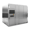
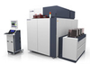
ASML Optics Lithography System TWINSCAN XT:450G

Description
The TWINSCAN XT:450G 365-nm Step-and-Scan system is a high productivity, dual-stage lithography tool designed for volume production of critical i-line applications down to 220-nm resolution and beyond. The dual wafer-stage technology of the TWINSCAN platform enables the exposure of one wafer and the alignment and mapping of the next wafer to take place in parallel, thereby virtually eliminating overhead time and allowing for continuous patterning of wafers. In addition, a high-intensity 5.5-kW Hg lamp and fast stages ensure maximum productivity by minimizing the exposure scanning time per field and the stepping time between fields. The level sensor, in combination with the TWINSCAN leveling approach, virtually eliminates differences between inner die and edge die and ensures high yield across the entire 300-mm wafer. High throughput and yield are combined with fast reticle exchange times and Lot Streaming to provide the lowest cost of operation. The tool’s excellent overlay and imaging capabilities allow non-critical KrF layers to be transformed to i-line, resulting in significant cost savings.
Description
The TWINSCAN XT:450G 365-nm Step-and-Scan system is a high productivity, dual-stage lithography tool designed for volume production of critical i-line applications down to 220-nm resolution and beyond. The dual wafer-stage technology of the TWINSCAN platform enables the exposure of one wafer and the alignment and mapping of the next wafer to take place in parallel, thereby virtually eliminating overhead time and allowing for continuous patterning of wafers. In addition, a high-intensity 5.5-kW Hg lamp and fast stages ensure maximum productivity by minimizing the exposure scanning time per field and the stepping time between fields. The level sensor, in combination with the TWINSCAN leveling approach, virtually eliminates differences between inner die and edge die and ensures high yield across the entire 300-mm wafer. High throughput and yield are combined with fast reticle exchange times and Lot Streaming to provide the lowest cost of operation. The tool’s excellent overlay and imaging capabilities allow non-critical KrF layers to be transformed to i-line, resulting in significant cost savings.

Suppliers

Company
Product
Description
Supplier Links
Lithography System - TWINSCAN XT:450G - ASML Optics
Wilton, CT, USA
Lithography System
TWINSCAN XT:450G
Lithography System TWINSCAN XT:450G
The TWINSCAN XT:450G 365-nm Step-and-Scan system is a high productivity, dual-stage lithography tool designed for volume production of critical i-line applications down to 220-nm resolution and beyond. The dual wafer-stage technology of the TWINSCAN platform enables the exposure of one wafer and the alignment and mapping of the next wafer to take place in parallel, thereby virtually eliminating overhead time and allowing for continuous patterning of wafers. In addition, a high-intensity 5.5-kW Hg lamp and fast stages ensure maximum productivity by minimizing the exposure scanning time per field and the stepping time between fields. The level sensor, in combination with the TWINSCAN leveling approach, virtually eliminates differences between inner die and edge die and ensures high yield across the entire 300-mm wafer. High throughput and yield are combined with fast reticle exchange times and Lot Streaming to provide the lowest cost of operation. The tool’s excellent overlay and imaging capabilities allow non-critical KrF layers to be transformed to i-line, resulting in significant cost savings.

The TWINSCAN XT:450G 365-nm Step-and-Scan system is a high productivity, dual-stage lithography tool designed for volume production of critical i-line applications down to 220-nm resolution and beyond. The dual wafer-stage technology of the TWINSCAN platform enables the exposure of one wafer and the alignment and mapping of the next wafer to take place in parallel, thereby virtually eliminating overhead time and allowing for continuous patterning of wafers.
In addition, a high-intensity 5.5-kW Hg lamp and fast stages ensure maximum productivity by minimizing the exposure scanning time per field and the stepping time between fields. The level sensor, in combination with the TWINSCAN leveling approach, virtually eliminates differences between inner die and edge die and ensures high yield across the entire 300-mm wafer. High throughput and yield are combined with fast reticle exchange times and Lot Streaming to provide the lowest cost of operation.
The tool’s excellent overlay and imaging capabilities allow non-critical KrF layers to be transformed to i-line, resulting in significant cost savings.

Supplier's Site

Technical Specifications

  ASML Optics
Product Category Lithography Equipment
Product Number TWINSCAN XT:450G
Product Name Lithography System
Unlock Full Specs
to access all available technical data

Similar Products